JAJSCH6C June   2016  – June 2021 TPS62135

PRODUCTION DATA  

  1. 特長
  2. アプリケーション
  3. 概要
  4. Revision History
  5. Device Comparison Table
  6. Pin Configuration and Functions
  7. Specifications
    1. 7.1 Absolute Maximum Ratings
    2. 7.2 ESD Ratings
    3. 7.3 Recommended Operating Conditions
    4. 7.4 Thermal Information
    5. 7.5 Electrical Characteristics
    6. 7.6 Typical Characteristics
  8. Parameter Measurement Information
    1. 8.1 Schematic
  9. Detailed Description
    1. 9.1 Overview
    2. 9.2 Functional Block Diagram
    3. 9.3 Feature Description
      1. 9.3.1 Precise Enable
      2. 9.3.2 Power Good (PG)
      3. 9.3.3 Pin-Selectable Output Voltage (VSEL and FB2)
      4. 9.3.4 MODE
      5. 9.3.5 Undervoltage Lockout (UVLO)
      6. 9.3.6 Thermal Shutdown
    4. 9.4 Device Functional Modes
      1. 9.4.1 Pulse Width Modulation (PWM) Operation
      2. 9.4.2 Power Save Mode Operation (PWM/PFM)
      3. 9.4.3 100% Duty-Cycle Operation
      4. 9.4.4 HICCUP Current Limit And Short Circuit Protection (TPS62135 only)
      5. 9.4.5 Current Limit And Short Circuit Protection (TPS621351 only)
      6. 9.4.6 Soft-Start / Tracking (SS/TR)
      7. 9.4.7 Output Discharge Function (TPS62135 only)
      8. 9.4.8 Starting into a Pre-Biased Load (TPS621351 only)
  10. 10Application and Implementation
    1. 10.1 Application Information
      1. 10.1.1 Programming the Output Voltage
      2. 10.1.2 External Component Selection
      3. 10.1.3 Inductor Selection
      4. 10.1.4 Capacitor Selection
        1. 10.1.4.1 Output Capacitor
        2. 10.1.4.2 Input Capacitor
        3. 10.1.4.3 Soft-Start Capacitor
      5. 10.1.5 Tracking Function
      6. 10.1.6 Output Filter and Loop Stability
    2. 10.2 Typical Applications
      1. 10.2.1 Typical Application with Adjustable Output Voltage
        1. 10.2.1.1 Design Requirements
        2. 10.2.1.2 Detailed Design Procedure
        3. 10.2.1.3 Application Curves
      2. 10.2.2 Typical Application using VSEL and FB2
        1. 10.2.2.1 Design Requirements
        2. 10.2.2.2 Detailed Design Procedure
        3. 10.2.2.3 Application Curves
    3. 10.3 System Examples
      1. 10.3.1 LED Power Supply
      2. 10.3.2 Powering Multiple Loads
      3. 10.3.3 Voltage Tracking
      4. 10.3.4 Precise Soft-Start Timing
  11. 11Power Supply Recommendations
  12. 12Layout
    1. 12.1 Layout Guidelines
    2. 12.2 Layout Example
    3. 12.3 Thermal Considerations
  13. 13Device and Documentation Support
    1. 13.1 Device Support
      1. 13.1.1 Third-Party Products Disclaimer
    2. 13.2 Receiving Notification of Documentation Updates
    3. 13.3 サポート・リソース
    4. 13.4 Trademarks
    5. 13.5 静電気放電に関する注意事項
    6. 13.6 用語集
  14. 14Mechanical, Packaging, and Orderable Information

パッケージ・オプション

メカニカル・データ(パッケージ|ピン)
サーマルパッド・メカニカル・データ
発注情報

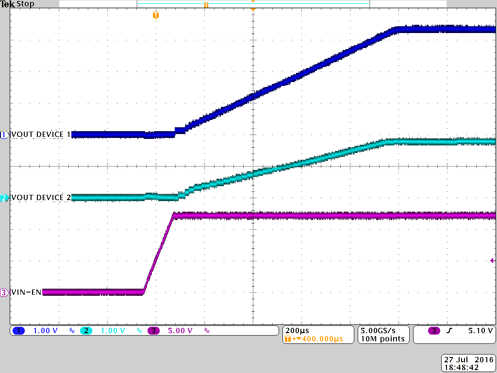
Voltage Tracking

DEVICE 2 follows the voltage applied to the SS/TR pin. A ramp on SS/TR to 0.7 V ramps the output voltage according to the 0.7 V reference.

Tracking the 3.3 V of DEVICE 1 requires a resistor divider on SS/TR of DEVICE 2 equal to the output voltage divider of DEVICE 1. The output current of 2.5µA from the SS/TR pin cases an offset voltage on the resistor divider formed by R5 and R6. The equivalent resistance of R6 // R5 should therefore be kept below 15kΩ.

GUID-1C8CC6E7-3473-4798-A21A-6B2DBBFD2AEB-low.gifFigure 10-85 Tracking Example
GUID-33835313-B730-43B7-BE59-5EB95D8C7A0C-low.pngFigure 10-86 Tracking