-
TPS62152-Q1 Automotive Wide Input, Fixed 3-V Output Voltage, 1-A Step-Down Converter in 3 × 3-mm QFN Package
- 1 Features
- 2 Applications
- 3 Description
- 4 Revision History
- 5 Pin Configuration and Functions
- 6 Specifications
-
7 Detailed Description
- 7.1 Overview
- 7.2 Functional Block Diagram
- 7.3
Feature Description
- 7.3.1 Pulse-Width Modulation (PWM) Operation
- 7.3.2 100% Duty-Cycle Operation
- 7.3.3 Enable / Shutdown (EN)
- 7.3.4 Soft Start or Tracking (SS/TR)
- 7.3.5 Current-Limit and Short-Circuit Protection
- 7.3.6 Power Good (PG)
- 7.3.7 Pin-Selectable Output Voltage (DEF)
- 7.3.8 Frequency Selection (FSW)
- 7.3.9 Undervoltage Lockout (UVLO)
- 7.3.10 Thermal Shutdown
- 7.3.11 Tracking Function
- 7.3.12 Feedback Pin (FB)
- 7.4 Device Functional Modes
- 8 Application and Implementation
- 9 Power Supply Recommendations
- 10Layout
- 11Device and Documentation Support
- 12Mechanical, Packaging, and Orderable Information
- IMPORTANT NOTICE
パッケージ・オプション
デバイスごとのパッケージ図は、PDF版データシートをご参照ください。
メカニカル・データ(パッケージ|ピン)
- RGT|16
サーマルパッド・メカニカル・データ
発注情報
TPS62152-Q1 Automotive Wide Input, Fixed 3-V Output Voltage, 1-A Step-Down Converter in 3 × 3-mm QFN Package
1 Features
- Qualified for Automotive Applications
- AEC-Q100 Qualified With the Following Results:
- DCS-Control Topology
- Input Voltage Range: 4 V to 17 V
- Up to 1-A Output Current
- Fixed Output Voltage: 3.3 V
- Programmable Soft Start and Tracking
- Seamless Power-Save Mode Transition
- Quiescent Current of 17 µA (Typ.)
- Selectable Operating Frequency
- Power-Good Output
- 100% Duty-Cycle Mode
- Short-Circuit Protection
- Overtemperature Protection
- Available in a 3-mm × 3-mm, VQFN-16 Package
2 Applications
- Automotive Infotainment and Cluster
- Instrument Cluster
- Center Stack
- Head Unit
- Rear-Seat Entertainment
- Advanced Driver-Assistance System (ADAS)
- Surround View
- Rear-View Camera
- Front Camera
3 Description
The TPS62152-Q1 device is an easy-to-use
synchronous step-down dc-dc converter optimized for applications with high power density and features a fixed 3.3-V output with a current capability of up to
1 A. A high switching frequency of 2.5 MHz (typical) allows the use of small inductors and provides fast transient response as well as high output-voltage accuracy by use of the DCS-Control topology.
With a wide operating input voltage range of 4 V to 17 V, the device is ideally suited for systems powered from either a Li-Ion or other batteries as well as from 12-V intermediate power rails.
The soft-start pin controls the output voltage start-up ramp, which allows operation either as a standalone power supply or in tracking configurations. Power sequencing is also possible by configuring the enable and open-drain power-good pins.
In power-save mode, the device draws quiescent current of about 17 μA from VIN. Power-save mode, entered automatically and seamlessly if the load is small, maintains high efficiency over the entire load range. Entering shutdown mode turns the device off, and shutdown current consumption is less than 2 μA.
The device package is a 16-pin VQFN measuring
3-mm × 3-mm (RGT) and has an exposed thermal pad for better thermal performance.
Device Information(1)
| PART NUMBER | PACKAGE | BODY SIZE (NOM) |
|---|---|---|
| TPS62152-Q1 | VQFN (16) | 3.00 mm × 3.00 mm |
- For all available packages, see the orderable addendum at the end of the datasheet.
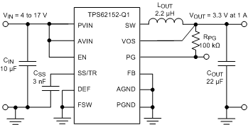
Typical Application
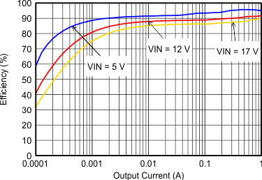
Efficiency Vs Output Current
4 Revision History
Changes from A Revision (July 2013) to B Revision
- Changed output voltage in the Features sectionGo
- Changed output voltage in second paragraph of the Description sectionGo
- Added the ESD Ratings table, Feature Description section, Programming section, Application and Implementation section, Layout section, Device and Documentation Support section, and Mechanical, Packaging, and Orderable Information sectionGo
- Changed the minimum supply voltage value from 3 to 4 in the Recommended Operating Conditions table Go
- Added the capacitor and inductor parameters to the Recommended Operating Conditions tableGo
- Changed the minimum input voltage value from 3 to 4 in the Electrical Characteristics table Go
- Deleted all references to the TPS62150-Q1 device and adjustable output versionsGo
- Changed the values of the output voltage range parameter in the Electrical Characteristics from 0.9 (min) and 6 (max) to 3.3 (typ) Go
- Added inductor and capacitor values to some of the graphs in the Typical Characteristics sectionGo
- Deleted empty rows 0.47 µH and 4.7 µH and columns for 4.7 µF and 400 µF from the L-C Output Filter Combinations tableGo
Changes from * Revision (July 2013) to A Revision
5 Pin Configuration and Functions
Pin Functions
| PIN(1) | TYPE(2) | DESCRIPTION | |
|---|---|---|---|
| NAME | NO. | ||
| AGND | 6 | G | Analog ground. Connected AGND directly to the exposed thermal pad and common ground plane. |
| AVIN | 10 | S | Supply voltage for control circuitry. Connect to the same source as PVIN. |
| DEF | 8 | I | Output voltage scaling (Low = nominal, High = nominal + 5%)(4) |
| EN | 13 | I | Enable input (High = enabled, Low = disabled)(4) |
| FB | 5 | I | TI recommends connecting FB to AGND for improved thermal performance. |
| FSW | 7 | I | Switching frequency select (Low ≈ 2.5 MHz, High ≈ 1.25 MHz(3) for typical operation)(4) |
| PG | 4 | O | Output power good (High = VOUT ready, Low = VOUT below nominal regulation); open drain (requires pullup resistor; goes high-impedance when device is switched off) |
| PGND | 15 | G | Power ground. Must be connected directly to the exposed thermal pad and common ground plane. |
| 16 | |||
| PVIN | 11 | S | Supply voltage for power stage. Connect to same source as AVIN. |
| 12 | |||
| SS/TR | 9 | I | Soft-start or tracking pin. An external capacitor connected to this pin sets the internal voltage-reference rise time. The pin can be used for tracking and sequencing. |
| SW | 1 | O | Switch node, which is connected to the internal MOSFET switches. Connect inductor between SW and output capacitor. |
| 2 | |||
| 3 | |||
| VOS | 14 | I | Output-voltage sense pin and connection for the control-loop circuitry. |
| Exposed thermal pad | — | Connect to AGND (pin 6), PGND (pins 15,16) and common ground plane(5). Solder to PCB to achieve appropriate power dissipation and mechanical reliability. | |
6 Specifications
6.1 Absolute Maximum Ratings
over operating free-air temperature range (unless otherwise noted)(1)| MIN | MAX | UNIT | ||
|---|---|---|---|---|
| Pin voltage range(2) | AVIN, PVIN | –0.3 | 20 | V |
| EN, SS/TR | –0.3 | VIN + 0.3 | ||
| SW | –0.3 | VIN + 0.3 | ||
| DEF, FSW, FB, PG, VOS | –0.3 | 7 | ||
| Power-good sink current | PG | 10 | mA | |
| Operating junction temperature, TJ | –40 | 125 | °C | |
| Storage temperature, Tstg | –65 | 150 | °C | |
6.2 ESD Ratings
| VALUE | UNIT | ||||
|---|---|---|---|---|---|
| V(ESD) | Electrostatic discharge | Human body model (HBM), per AEC Q100-002(1) | ±2000 | V | |
| Charged device model (CDM), per AEC Q100-011 | All pins | ±500 | |||
| Corner pins (1, 4, 5, 8, 9, 12, 13, 16) | ±750 | ||||
6.3 Recommended Operating Conditions
over operating free-air temperature range (unless otherwise noted)| MIN | MAX | UNIT | |||
|---|---|---|---|---|---|
| VIN | Supply voltage at AVIN and PVIN(1) | 4 | 17 | V | |
| CIN | Input filter capacitor | 10 | µF | ||
| COUT | Output buffer capacitor | 10 | µF | ||
| LOUT | Output inductor | 1 | 3.3 | µH | |
| TA | Operating free air temperature | –40 | 125 | °C | |
6.4 Thermal Information
| THERMAL METRIC(1) | TPS62152-Q1 | UNIT | |
|---|---|---|---|
| RGT (VQFN) | |||
| 16 Pins | |||
| RθJA | Junction-to-ambient thermal resistance | 45 | °C/W |
| RθJC(top) | Junction-to-case (top) thermal resistance | 51.6 | °C/W |
| RθJB | Junction-to-board thermal resistance | 17.4 | °C/W |
| ψJT | Junction-to-top characterization parameter | 0.9 | °C/W |
| ψJB | Junction-to-board characterization parameter | 17.4 | °C/W |
| RθJC(bot) | Junction-to-case (bottom) thermal resistance | 4.4 | °C/W |
6.5 Electrical Characteristics
over free-air temperature range (TA= –40°C to 125°C), typical values at VIN = AVIN = PVIN = 12 V and TA = 25°C (unless otherwise noted)| PARAMETER | TEST CONDITIONS | MIN | TYP | MAX | UNIT | ||
|---|---|---|---|---|---|---|---|
| SUPPLY | |||||||
| VIN | Input voltage range(1) | 4 | 17 | V | |||
| IQ | Operating quiescent current | EN = High, IOUT = 0 mA, device not switching | 17 | 25 | µA | ||
| ISD | Shutdown current(2) | EN = Low | 1.5 | 4 | µA | ||
| VUVLO | Undervoltage lockout threshold | Falling input voltage | 2.6 | 2.7 | 2.8 | V | |
| Hysteresis | 200 | mV | |||||
| TSD | Thermal shutdown temperature | 160 | °C | ||||
| Thermal shutdown hysteresis | 20 | °C | |||||
| CONTROL (EN, DEF, FSW, SS/TR, PG) | |||||||
| VH | High-level input threshold voltage (EN, DEF, FSW) | 0.9 | V | ||||
| VL | Low-level input threshold voltage (EN, DEF, FSW) | 0.3 | V | ||||
| ILKG | Input leakage current (EN, DEF, FSW) | EN = VIN or GND; DEF, FSW = VOUT or GND | 0.01 | 1 | µA | ||
| VTH_PG | Power-good threshold voltage | Rising (%VOUT) | 92% | 95% | 98% | ||
| Falling (%VOUT) | 87% | 90% | 94% | ||||
| VOL_PG | Power-good output low | IPG = –2 mA | 0.07 | 0.3 | V | ||
| ILKG_PG | Input leakage current (PG) | VPG = 1.8 V | 1 | 400 | nA | ||
| ISS/TR | SS/TR pin source current | 2.3 | 2.5 | 2.7 | µA | ||
| POWER SWITCH | |||||||
| RDS(ON) | High-side MOSFET on-resistance | VIN ≥ 6 V | 90 | 170 | mΩ | ||
| VIN = 3 V | 120 | ||||||
| Low-side MOSFET on-resistance | VIN ≥ 6 V | 40 | 70 | ||||
| VIN = 3 V | 50 | ||||||
| ILIMF | High-side MOSFET forward current limit(3) | VIN = 12 V, TA= 25°C | 1.4 | 1.7 | 2.2 | A | |
| OUTPUT | |||||||
| VREF | Internal reference voltage(4) | 0.8 | V | ||||
| ILKG_FB | Input leakage current (FB) | VFB = 0.8 V | 1 | 100 | nA | ||
| VOUT | Output voltage range | VIN ≥ VOUT | 3.3 | V | |||
| DEF (Output voltage programming) | DEF = 0 (GND) | VOUT | V | ||||
| DEF = 1 (VOUT) | VOUT + 5% | ||||||
| Initial output voltage accuracy(5) | PWM mode operation, VIN ≥ VOUT + 1 V | –1.8% | 1.8% | ||||
| Power-save mode operation, COUT = 22 µF | –2.3% | 2.8% | |||||
| Load regulation(6) | VIN = 12 V, VOUT = 3.3 V, PWM mode operation | 0.05 | %/A | ||||
| Line regulation(6) | 3 V ≤ VIN ≤ 17 V, VOUT = 3.3 V, IOUT = 1 A, PWM mode operation | 0.02 | %/V | ||||
6.6 Typical Characteristics
Table 1. Table of Graphs
| DESCRIPTION | FIGURE | ||
|---|---|---|---|
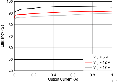
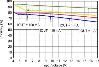
| Efficiency | vs Output Current | Figure 1, Figure 3 | |
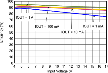
| vs Input Voltage | Figure 2, Figure 4 | ||
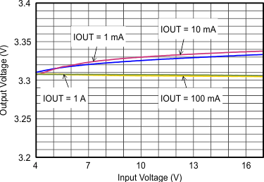
| Output Voltage Accuracy | Load Regulation | Figure 5 | |
| Line Regulation | Figure 6 | ||
| Switching Frequency | vs Input Voltage | Figure 7 | |
| vs Output Current | Figure 8 | ||
| Input Quiescent Current | vs Input voltage | Figure 9 | |
| Input Shutdown Current | vs Input voltage | Figure 10 | |
| High-Side Static Drain-Source-Resistance (RDSon) | vs Input voltage | Figure 11 | |
| Low-Side Static Drain-Source-Resistance (RDSon) | vs Input voltage | Figure 12 | |
| Output Voltage Ripple | vs Output Current | Figure 13 | |
| Output Current | vs Input Voltage | Figure 14 | |
| Power-Supply Rejection Ratio | vs Frequency | Figure 15, Figure 16 | |
| PWM-PSM-Transition | Figure 17 | ||
| Load Transient Response | Figure 18 | ||
| Load Transient Response | Rising Edge | Figure 19 | |
| Falling Edge | Figure 20 | ||
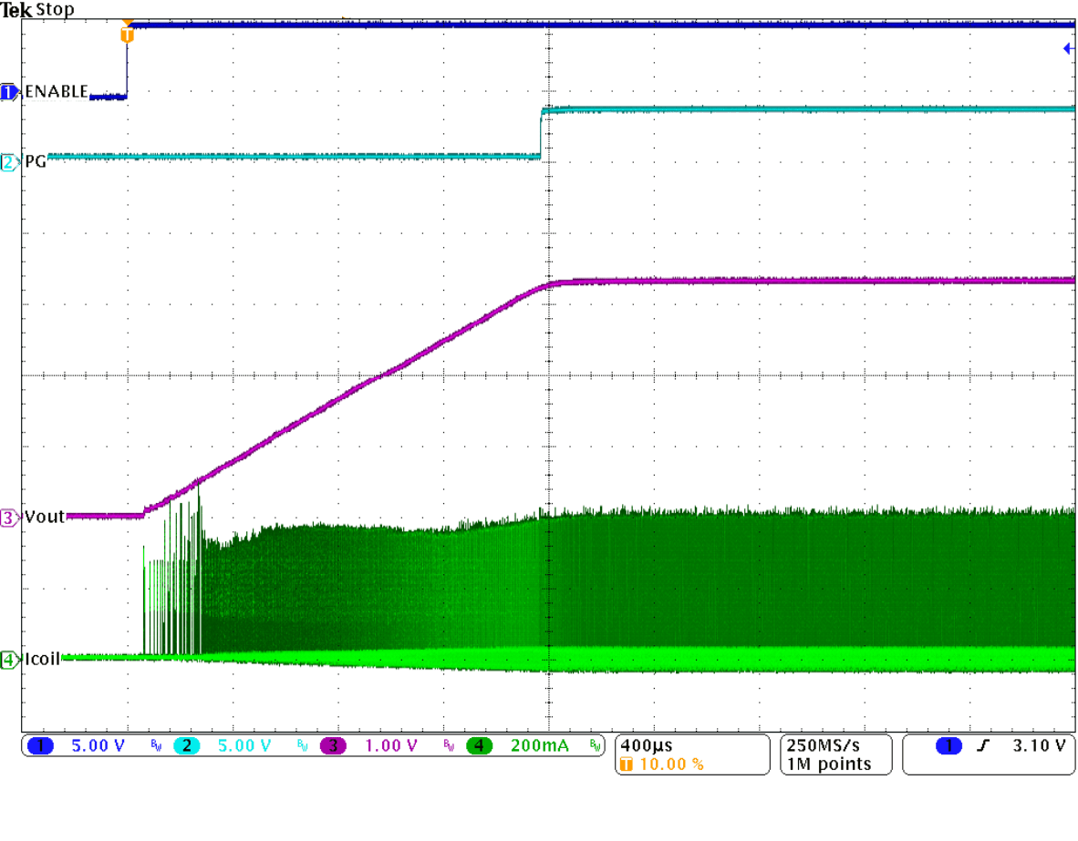
| Startup | Into 100 mA | Figure 21 | |
| Into 1 A | Figure 22 | ||
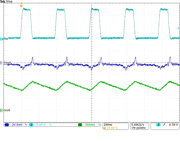
| Typical Operation in PWM Mode | Figure 23 | ||
| Typical Operation in Power Save Mode | Figure 24 | ||
| FSW = 1.25 MHz | L = 2.2 µH (XFL4020) | COUT = 22 µF |
| CIN = 10 µF |
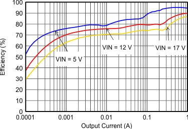
| FSW = 2.5 MHz | L = 2.2 µH (XFL4020) | COUT = 22 µF |
| CIN = 10 µF |
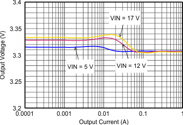
| L = 2.2 µH (XFL4020) | COUT = 22 µF | CIN = 10 µF |
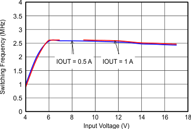
| L = 2.2 µH (XFL4020) | COUT = 22 µF | CIN = 10 µF |
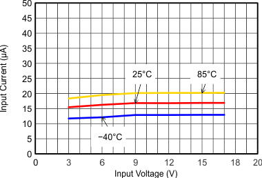
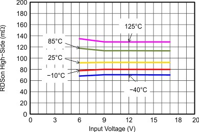
vs Input Voltage
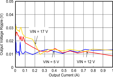
| L = 2.2 µH (XFL4020) | COUT = 22 µF | CIN = 10 µF |
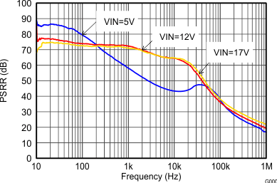
| FSW = 2.5 MHz | L = 2.2 µH (XFL4020) | COUT = 22 µF |
| CIN = 10 µF |
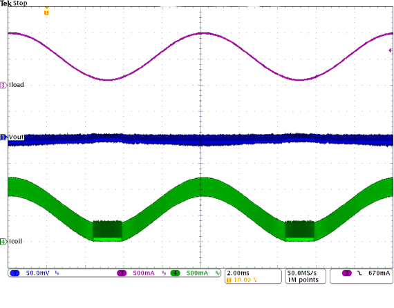
| VIN = 12 V With 50 mV/div | ||
| VIN = 12 V | ||
| IOUT = 1 A |
| FSW = 2.5 MHz | L = 2.2 µH (XFL4020) | COUT = 22 µF |
| CIN = 10 µF |
| L = 2.2 µH (XFL4020) | COUT = 22 µF | CIN = 10 µF |
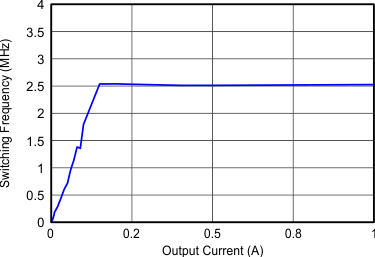
| FSW = Low | L = 2.2 µH (XFL4020) | COUT = 22 µF |
| CIN = 10 µF |
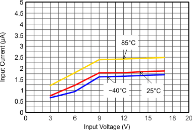
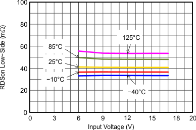
vs Input Voltage
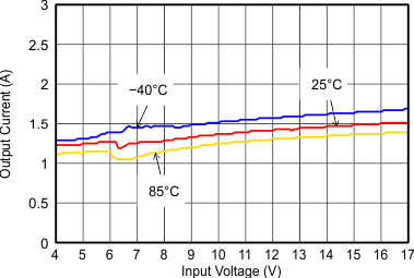
| L = 2.2 µH (XFL4020) | COUT = 22 µF | CIN = 10 µF |
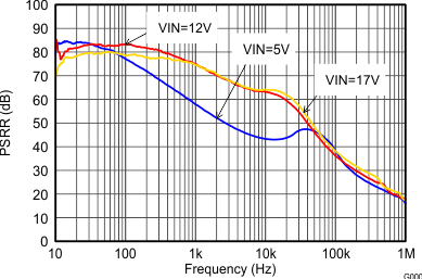
| FSW = 2.5 MHz | L = 2.2 µH (XFL4020) | COUT = 22 µF |
| CIN = 10 µF |
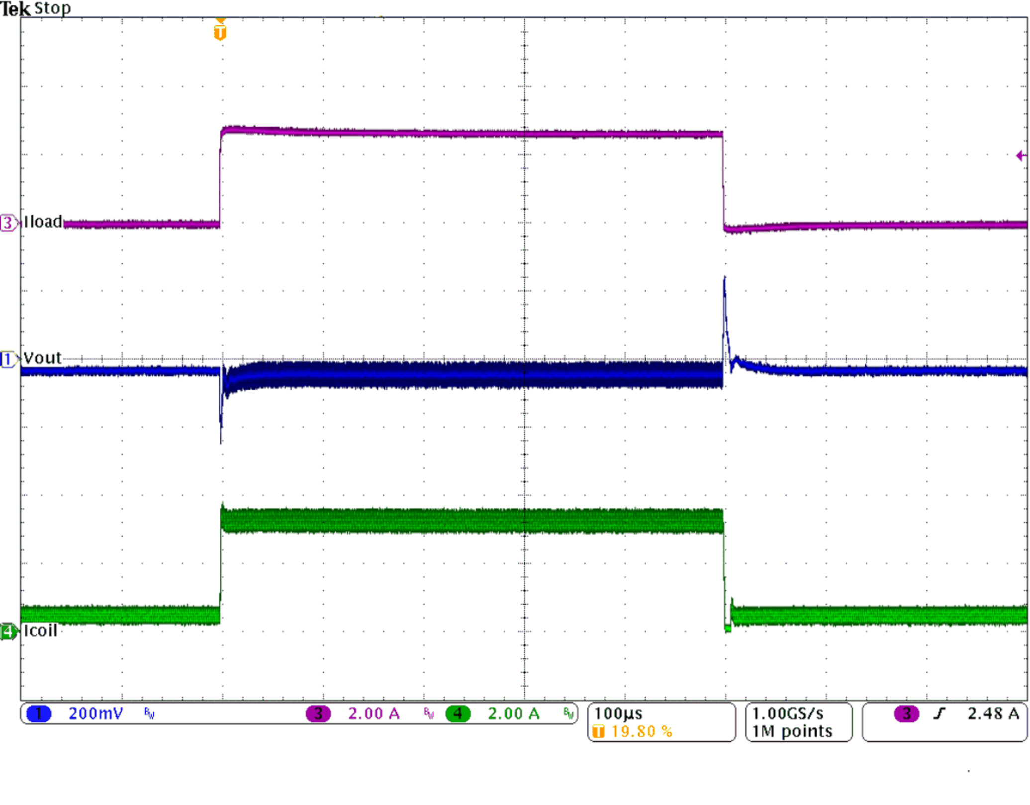
| VIN = 12 V | IOUT = 0 to 5 A and back to 0 A | |
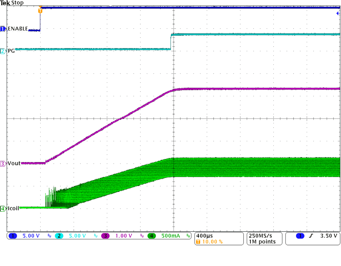
| VIN = 12 V | ||
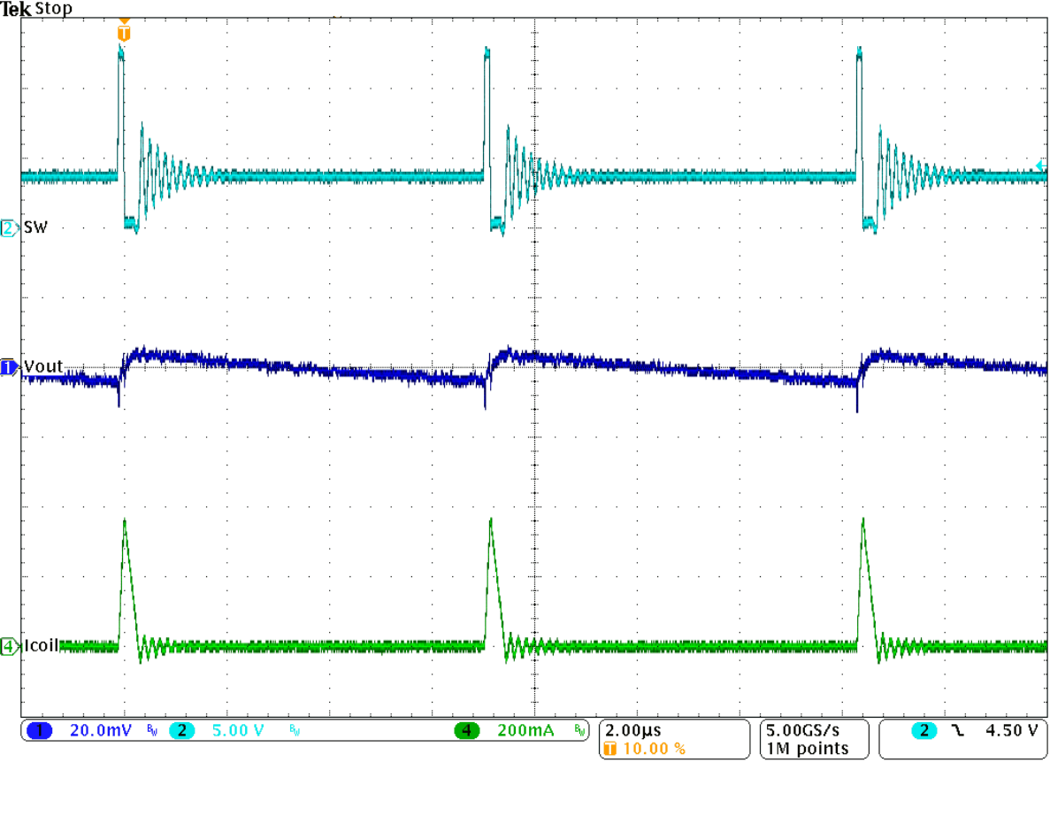
| IOUT = 10 mA |
7 Detailed Description
7.1 Overview
The base for the TPS62152-Q1 synchronous switched-mode power converters is the DCS-Control™ topology (direct control with seamless transition into power-save mode), an advanced regulation topology that combines the advantages of hysteretic, voltage-mode and current mode control including an ac loop directly associated to the output voltage. This control loop takes information about output voltage changes and feeds it directly to a fast comparator stage. The control loop sets the switching frequency, which is constant for steady-state operating conditions, and provides immediate response to dynamic load changes. A voltage feedback loop obtains accurate dc load regulation. The internally compensated regulation network achieves fast and stable operation with small external components and low-ESR capacitors.
The DCS-Control topology supports pulse-width modulation (PWM) mode for medium and heavy load conditions and a power save-mode at light loads. During PWM, the device operates at the nominal switching frequency in continuous-conduction mode. This frequency is typically about 2.5 MHz, with a controlled frequency variation depending on the input voltage. If the load current decreases, the converter enters power-save mode to sustain high efficiency down to very light loads. In power-save mode, the switching frequency decreases linearly with the load current. Because DCS-Control topology supports both operation modes within one single building block, the transition from PWM to power-save mode is seamless, without effects on the output voltage.
Because the TPS62152-Q1 device has a fixed output voltage of 3.3 V, the device provide smallest solution size and lowest current consumption, requiring only three external components. An internal current limit supports nominal output currents of up to 1 A.
The TPS62152-Q1 device offers both excellent dc voltage and superior load-transient regulation, combined with very low output-voltage ripple, minimizing interference with RF circuits.
7.2 Functional Block Diagram

7.3 Feature Description
7.3.1 Pulse-Width Modulation (PWM) Operation
The TPS62152-Q1 device operates with pulse-width modulation in continuous conduction mode (CCM) with a nominal switching frequency of 2.5 MHz or 1.25 MHz, selectable with the FSW pin. The frequency variation in PWM is controlled and depends on VIN, VOUT and the inductance. The device operates in PWM mode as long the output current is higher than half the inductor ripple current. To maintain high efficiency at light loads, the device enters power-save mode at the boundary to discontinuous-conduction mode (DCM). This happens if the output current becomes smaller than half the inductor ripple current.
7.3.2 100% Duty-Cycle Operation
D = VOUT / VIN gives the duty cycle of the buck converter, which increases as the input voltage comes close to the output voltage. In this case, the device starts 100% duty-cycle operation, turning on the high-side switch 100% of the time. The high-side switch stays turned on as long as the output voltage is below the internal set point. This allows the conversion of small input-to-output voltage differences, for example, for longest operation time of battery-powered applications. In 100% duty-cycle mode, the low-side FET switches off.
The calculation for minimum input voltage to maintain output voltage regulation, depending on the load current and the output voltage level, is:

where
- IOUT is the output current
- RDS(on) is the on resistance of the high-side FET
- RL is the DC resistance of the inductor used
7.3.3 Enable / Shutdown (EN)
Setting enable (EN) High starts operation of the device.
Pulling EN Low forces shutdown, with a shutdown current of typically 1.5 µA. The shutdown state turns off the internal power MOSFETs as well as the entire control circuitry. The internal resistive divider pulls down the output voltage smoothly. An internal pulldown resistor of about 400 kΩ is connected and keeps EN logic low, if the pin is floating. Driving the pin High disconnects the pulldown.
Connecting the EN pin to an appropriate output signal of another power rail provides sequencing of multiple power rails.
7.3.4 Soft Start or Tracking (SS/TR)
The internal soft-start circuitry controls the output voltage slope during start-up. This control avoids excessive inrush current, ensures a controlled output-voltage rise time, and prevents unwanted voltage drops from high-impedance power sources or batteries. On setting EN to start device operation, the device begins switching after a delay of about 50 µs and VOUT rises with a slope controlled by an external capacitor connected to the SS/TR pin. See Figure 21 and Figure 22 for typical start-up operation.
Connecting SS/TR directly to AVIN provides fastest start-up behavior. The TPS62152-Q1 device can start into a pre-biased output. During monotonic pre-biased start-up, neither power MOSFET turns on until the internal ramp of the device sets an output voltage above the pre-bias voltage. If EN = GND, setting the device to shutdown, or the device is in undervoltage lockout or thermal shutdown, an internal resistor pulls the SS/TR pin down to ensure a proper low level. Returning from those shutdown states causes a new start-up sequence as set by the SS/TR connection.
The device can track a master voltage supplied to SS/TR. The output voltage follows this voltage in both directions, up and down (see the Application Information section).
7.3.5 Current-Limit and Short-Circuit Protection
The TPS62152-Q1 device has protection against heavy loads and short-circuit events. At heavy loads, the current limit determines the maximum output current. On reaching the current limit, the high-side FET turns off. To avoid shoot-through current, the low-side FET switches on to sink the inductor current. The high-side FET turns on again only if the current in the low-side FET has decreased below the low-side current-limit threshold.
The current limit (see the Electrical Characteristics table) restricts the output current of the device. Because of internal propagation delay, the actual current can exceed the static current limit during this propagation delay time. The calculation for the dynamic current limit is as follows:

where
- ILIMF is the static current limit, specified in the Electrical Characteristics table
- VL is the voltage across the inductor (VIN – VOUT)
- L is the inductor value
- tPD is the internal propagation delay
The current limit can exceed static values, especially if the input voltage is high and the circuit uses very small inductances. The calculation for the peak current in the dynamic high-side switch is as follows:

7.3.6 Power Good (PG)
The TPS62152-Q1 device has a built-in power-good (PG) function to indicate whether the output voltage has reached its appropriate level or not. One use of the PG signal is for start-up sequencing of multiple rails. The PG pin is an open-drain output that requires a pullup resistor to any voltage below 7 V. The pin can sink 2 mA of current and maintain its specified logic-low level. The pin is high-impedance when EN, UVLO, or thermal shutdown turns the device off. The TPS62152-Q1 device features PG = Low in this case and can be used to actively discharge VOUT. The VIN voltage must remain present for the PG pin to stay Low.
7.3.7 Pin-Selectable Output Voltage (DEF)
Setting the DEF pin to High can increase the output voltage of the TPS62152-Q1 device by 5% above the nominal voltage (the maximum allowed voltage is 7 V; therefore, TI recommends connecting the DEF pin to VOUT or PG, not VIN). When DEF is Low, the device regulates to the nominal output voltage. Increasing the nominal voltage allows adapting the power supply voltage to the variations of the application hardware. See Voltage Margining Using the TPS62130, SLVA489, for detailed information on voltage margining using the TPS62152-Q1 device. A pulldown resistor of about 400 kΩ internally connects to the pin, to ensure a proper logic level if the pin is high-impedance or floating after initially set to Low. Setting the pin to High disconnects the resistor.
7.3.8 Frequency Selection (FSW)
To get high power density with a very small solution size, a high switching frequency allows the use of small external components for the output filter. However, switching losses increase with the switching frequency. If efficiency is the key parameter, more than solution size, set the switching frequency to half (1.25 MHz typical) by pulling FSW to High. It is mandatory to start with FSW = Low to limit inrush current. Connecting the pin to VOUT or PG is one way to ensure FSW = Low at start-up. Running with lower frequency achieves higher efficiency, but also creates higher output-voltage ripple. Pull FSW to Low for high frequency operation (2.5 MHz typical). To get low ripple and full output current at the lower switching frequency, TI recommends using an inductor of at least 2.2 µH. The device accommodates a change of switching frequency during operation, if needed. A pulldown resistor of about 400 kΩ internally connects to the pin, acting the same way as at the DEF pin (see Pin-Selectable Output Voltage (DEF)).
7.3.9 Undervoltage Lockout (UVLO)
If the input voltage drops, the undervoltage lockout prevents improper operation of the device by switching off both the power FETs. The typical setting of the undervoltage lockout threshold is 2.7 V. The device is fully operational for voltages above the UVLO threshold and turns off if the input voltage trips the threshold. The converter starts operation again once the input voltage exceeds the threshold by a hysteresis of typically 200 mV.
7.3.10 Thermal Shutdown
An internal temperature sensor monitors the junction temperature (TJ) of the device. If TJ exceeds 160°C (typ), the device goes into thermal shutdown. Both the high-side and low-side power FETs turn off, and PG goes into the high-impedance state. When TJ decreases below the hysteresis amount, the converter resumes normal operation, beginning with soft start. To avoid unstable conditions, the device implements a hysteresis of typically 20°C on the thermal shutdown temperature.
7.3.11 Tracking Function
For implementing a tracking function, use the SS/TR pin for this purpose by connecting it to an external tracking voltage. The output voltage tracks the external tracking voltage. If the tracking voltage is between 50 mV and
1.2 V, the FB pin tracks the SS/TR pin voltage as described in Equation 4 and shown in Figure 25.

 Figure 25. Voltage Tracking Relationship
When the SS/TR pin voltage reaches about 1.2 V, a clamp locks the internal voltage to the internal feedback voltage, and the device goes to normal regulation. This process works for rising and falling tracking voltages with the same behavior, as long as the input voltage is within the recommended operating conditions. For decreasing SS/TR pin voltage, the device does not sink current from the output. So, the resulting decrease of the output voltage may be slower than the SS/TR pin voltage if the load is light. When driving the SS/TR pin with an external voltage, do not exceed the voltage rating of the SS/TR pin, which is VIN + 0.3 V.
If the input voltage drops into undervoltage lockout or even down to zero, the output voltage goes to zero, independent of the tracking voltage. Figure 26 shows how to connect devices to get ratiometric and simultaneous sequencing by using the tracking function.
 Figure 26. Sequence for Ratiometric and Simultaneous Start-Up
The resistive divider of R1 and R2 can be used to change the ramp rate of VOUT2 faster, slower, or the same as VOUT1.
To achieve a sequential start-up, connect the PG pin of VOUT1 to the EN pin of VOUT2. A ratiometric start-up sequence happens if both supplies share the same soft-start capacitor. Equation 10 calculates the soft-start time, though this circuit arrangement requires doubling the SS/TR current. See TPS62130/40/50 Sequencing and Tracking, SLVA470, for details about these and other tracking and sequencing circuits.
NOTE
If the voltage at the FB pin is below its typical value of 0.8 V, the output voltage accuracy may have a wider tolerance than specified.
7.3.12 Feedback Pin (FB)
The FB pin is pulled down internally and may be left floating. Connecting to AGND to improve thermal resistance is recommended.
7.4 Device Functional Modes
7.4.1 Power-Save Mode Operation
If the load current decreases, the TPS62152-Q1 device enters the built-in power-save mode seamlessly. This transition secures a high efficiency in light load operation. The device remains in power-save mode as long as the inductor current is discontinuous.
In power-save mode, the switching frequency decreases linearly with the load current, maintaining high efficiency. The transition into and out of power-save mode happens within the entire regulation scheme and is seamless in both directions.
The TPS62152-Q1 device includes a fixed on-time circuitry. The calculation for estimated on-time, in steady-state operation, is:

For very small output voltages, the device keeps an absolute minimum on-time of about 80 ns to limit switching losses, thereby reducing the operating frequency from its nominal value, which keeps efficiency high. Use tON in Equation 6 to approximate the typical peak inductor current in power-save mode.

When VIN decreases to typically 15% above VOUT, the TPS62152-Q1 device does not enter power-save mode, regardless of the load current. The device maintains output regulation in PWM mode.
7.4.2 Active Output Discharge
The TPS62152A-Q1 pulls the PG pin Low, when the device is shut down by EN, UVLO, or thermal shutdown. Connecting PG to VOUT through a resistor can be used to discharge VOUT in those cases (see Figure 27). The discharge rate can be adjusted by RPG, which is also used to pull up the PG pin in normal operation. For reliability, keep the maximum current into the PG pin less than 10 mA.
 Figure 27. Active Output Discharge Through PG Pin
8 Application and Implementation
NOTE
Information in the following applications sections is not part of the TI component specification, and TI does not warrant its accuracy or completeness. TI’s customers are responsible for determining suitability of components for their purposes. Customers should validate and test their design implementation to confirm system functionality.
8.1 Application Information
The TPS62152-Q1 device is an automotive wide-input, synchronous step-down, DC-DC converter with a 3.3-V fixed output voltage and an output current of up to 1 A. The device can be used in buck-converter applications with an input range from 4 V to 17 V. The TPS62152-Q1 device is optimized for space constrained applications and consumes 17-µA (typical) current in power-save mode. Selectable switching frequency (1.25 MHz or 2.25 MHz) allows regulator design to be optimized for efficiency or solution size.
8.2 Typical Application
 Figure 28. 3.3-V, 1-A Power Supply
8.2.1 Design Requirements
The device is optimized for a certain range of output inductor and output capacitor values. See the Detailed Design Procedure section for details. The Recommended Operating Conditions table lists the allowed ranges for the input voltage, input buffer capacitor, output inductor, and output buffer capacitor. The values listed in this table must be followed when designing the regulator. Low-ESR ceramic capacitors should be used at the input and output for better filtering and ripple performance. The Detailed Design Procedure section provides the necessary equations and guidelines for selecting external components for this regulator.
8.2.2 Detailed Design Procedure
8.2.2.1 External Component Selection
The external components must fulfill the needs of the application, but also the stability criteria of the device control loop. Table 2 lists recommended components based on the schematic in Figure 28.
Table 2. List of Components
| REFERENCE | DESCRIPTION | MANUFACTURER |
|---|---|---|
| IC | 17-V, 1-A step-down converter, VQFN | TPS62152-Q1 RGT, Texas Instruments |
| LOUT | Inductor, 2.2-µH, 3.1-A, 0.165 in × 0.165 in (4,24 cm × 4,24 cm) | XFL4020-222MEB, Coilcraft |
| CIN | Capacitor, 10-µF, 25-V, ceramic | Standard |
| COUT | Capacitor, 22-µF, 6.3-V, ceramic | Standard |
| CSS | Capacitor, 3300-pF, 25-V, ceramic | |
| RPG | Resistor, 100 kΩ, chip, 0603, 1/16 W, 1% | Standard |
The TPS62152-Q1 works optimally within a range of external components. Consider the inductance and capacitance if the LC output filter in conjunction so as to create a double pole, responsible for the corner frequency of the converter (see the Output Filter and Loop Stability section). Use Table 3 to simplify the output-filter component selection.
Table 3. L-C Output Filter Combinations(1)
| 10 µF | 22 µF | 47 µF | 100 µF | 200 µF | |
|---|---|---|---|---|---|
| 1 µH | √ | √ | √ | √ | |
| 2.2 µH | √ | √(2) | √ | √ | √ |
| 3.3 µH | √ | √ | √ | √ |
The TPS62152-Q1 device can run with an inductor as low as 1 µH or 2.2 µH for the high-frequency setting (FSW = Low). However, for applications running with the low-frequency setting (FSW = High) or with low input voltages, 3.3 µH is a better recommendation. See Optimizing the TPS62130/40/50/60/70 Output Filter, SLVA463, for detailed information on further LC combinations.
8.2.2.1.1 Inductor Selection
Several effects like inductor ripple current, output ripple voltage, PWM-to-PSM transition point and efficiency affect the inductor selection. In addition, the inductor selected require rating for appropriate saturation current and dc resistance (DCR). Equation 7 and Equation 8 calculate the maximum inductor current under static load conditions.

where
- IL(max) is the maximum inductor current.
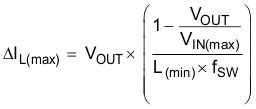
where
- L(min) is the minimum effective inductor value.
- fSW is the actual PWM switching frequency.
Calculating the maximum inductor current using the actual operating conditions gives the minimum required saturation current of the inductor. TI recommends adding a margin of about 20%. A larger inductor value is also useful to achieve lower ripple current, but increases the transient response time and may require a larger package. TI recommends the inductors listed in Table 4, which have worked successfully with the TPS62152-Q1.
Table 4. List of Inductors
| TYPE | INDUCTANCE [µH] |
SATURATION CURRENT [A](1) |
DIMENSIONS [L × W × H, mm] |
MANUFACTURER |
|---|---|---|---|---|
| XFL4020-222ME_ | 2.2 µH, ±20% | 3.5 | 4 × 4 × 2.1 | Coilcraft |
| XFL3012-222MEC | 2.2 µH, ±20% | 1.6 | 3 × 3 × 1.2 | Coilcraft |
| XFL3012-332MEC | 3.3 µH, ±20% | 1.4 | 3 × 3 × 1.2 | Coilcraft |
| VLS252012T-2R2M1R3 | 2.2 µH, ±20% | 1.3 | 2.5 × 2 × 1.2 | TDK |
| LPS3015-332 | 3.3 µH, ±20% | 1.4 | 3 × 3 × 1.4 | Coilcraft |
| 744025003 | 3.3 µH, ±20% | 1.5 | 2.8 × 2.8 × 2.8 | Wuerth |
| PSI25201B-2R2MS | 2.2 µH, ±20% | 1.3 | 2 × 2.5 × 1.2 | Cyntec |
| NR3015T-2R2M | 2.2 µH, ±20% | 1.5 | 3 × 3 × 1.5 | Taiyo Yuden |
The inductor value also determines the load current at which the device enters power-save mode as shown in Equation 9.

The designer can use Equation 8 to calculate the inductor value for changing this current level.
8.2.2.1.2 Output Capacitor
The recommended value for the output capacitor is 22 µF. The architecture of the TPS62152-Q1 device allows the use of ceramic output capacitors with low equivalent series resistance (ESR). These capacitors provide low output-voltage ripple and are ideal. To keep low resistance up to high frequencies and to get narrow capacitance variation with temperature, TI recommends using X7R or X5R dielectric. Using a higher value can have some advantages, such as smaller voltage ripple and a tighter DC output accuracy in power-save mode (see SLVA463).
NOTE
In power-save mode, the output-voltage ripple depends on the output capacitance and the ESR and peak inductor current of the capacitor. Using ceramic capacitors provides low ESR and low ripple.
8.2.2.1.2.1 Input Capacitor
For most applications, 10 µF is sufficient and recommended, though a larger value reduces input current ripple further. The input capacitor buffers the input voltage for transient events and also decouples the converter from the supply. TI recommends low-ESR multilayer ceramic capacitor for best filtering. Place the capacitor between PVIN and PGND as close as possible to those pins. Even though the AVIN and PVIN supply must come from the same input source, it is a good idea to place a capacitance of 0.1 µF from AVIN to AGND, to avoid potential noise coupling. Use of an RC low-pass filter from PVIN to AVIN is allowable but not mandatory.
8.2.2.1.2.2 Soft-Start Capacitor
A capacitance connected between SS/TR pin and AGND allows a user-programmable start-up slope of the output voltage. A constant-current source provides 2.5 µA to charge the external capacitance. Use Equation 10 to calculate the capacitance required for a given soft-start ramp time for the output voltage.

where
- CSS is the capacitance (F) required at the SS/TR pin
- tSS is the desired soft-start ramp time (s).
NOTE
DC bias effect: High-capacitance ceramic capacitors have a DC bias effect, which has a strong influence on the final effective capacitance. Therefore, choose the right capacitor value carefully. Package size and voltage rating in combination with dielectric material are responsible for differences between the rated capacitor value and the effective capacitance.
8.2.2.2 Output Filter and Loop Stability
The TPS62152-Q1 device has internal compensation to be stable with L-C filter combinations corresponding to a corner frequency calculated with Equation 11.

Table 3 gives proven and recommended nominal values for inductance and ceramic capacitance. Different values may work, but take care not to affect the loop stability. See Optimizing the TPS62130/40/50/60/70 Output Filter, SLVA463, for more information, including a detailed L-C stability matrix.
The TPS62152-Q1 device includes an internal 25-pF feedforward capacitor, connected between the VOS and FB pins. This capacitor impacts the frequency behavior and sets a pole and zero in the control loop with the resistors of the feedback divider, according to equations Equation 12 and Equation 13.


Though the TPS62152-Q1 device is stable without the pole and zero being in a particular location, adjusting their location to the specific needs of the application can provide better performance in power-save mode and/or improved transient response. An external feedforward capacitor can also be added. The application reports Optimizing Transient Response of Internally Compensated dc-dc Converters With Feedforward Capacitor, SLVA289, and Using a Feedforward Capacitor to Improve Stability and Bandwidth of TPS62130/40/50/60/70, SLVA466, provide a more-detailed discussion on the optimization for stability vs transient response.
8.2.3 Application Curves
 Figure 29. PWM-PSM-Transition
for VIN = 12 V With 50 mV/div
 Figure 30. Load Transient Response for VIN = 12 V and
IOUT= 0 A to 2.5 A and back to 0 A
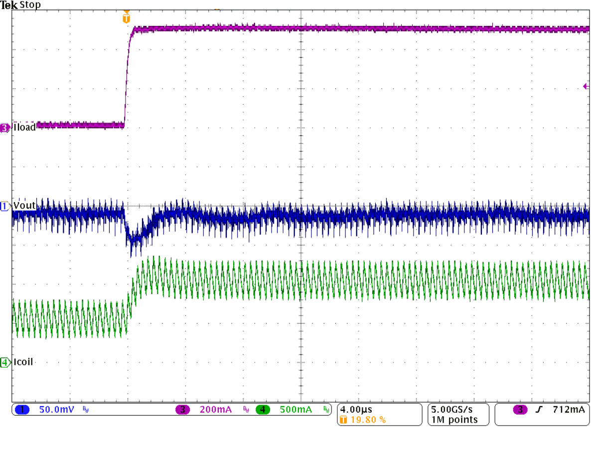 Figure 31. Load Transient Response of Figure 30,
Rising Edge
 Figure 33. Startup into 100 mA for VIN = 12 V
 Figure 35. Typical Operation in PWM Mode With IOUT = 1 A
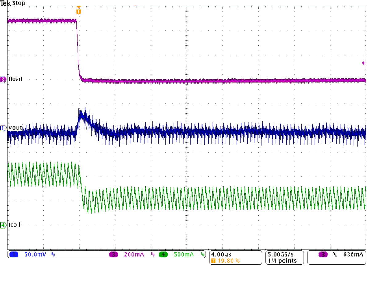 Figure 32. Load Transient Response of Figure 30,
Falling Edge
 Figure 34. Startup into 1 A for VIN = 12 V
 Figure 36. Typical Operation in Power Save Mode
With IOUT = 10 mA
