SLVSBB8B August 2014 – May 2017 TPS62180 , TPS62182
PRODUCTION DATA.
- 1 Features
- 2 Applications
- 3 Description
- 4 Revision History
- 5 Device Comparison Table
- 6 Pin Configuration and Functions
- 7 Specifications
-
8 Detailed Description
- 8.1 Overview
- 8.2 Functional Block Diagram
- 8.3 Feature Description
- 8.4
Device Functional Modes
- 8.4.1 Pulse Width Modulation (PWM) Operation
- 8.4.2 Power Save Mode (PSM) Operation
- 8.4.3 Minimum Duty Cycle and 100% Mode Operation
- 8.4.4 Automatic Efficiency Enhancement (AEE)
- 8.4.5 Phase-Shifted Operation
- 8.4.6 Current Limit, Current Balancing, and Short Circuit Protection
- 8.4.7 Tracking
- 8.4.8 Operation with Fixed VOUT
- 9 Application and Implementation
- 10Power Supply Recommendations
- 11Layout
- 12Device and Documentation Support
- 13Mechanical, Packaging, and Orderable Information
9 Application and Implementation
NOTE
Information in the following applications sections is not part of the TI component specification, and TI does not warrant its accuracy or completeness. TI’s customers are responsible for determining suitability of components for their purposes. Customers should validate and test their design implementation to confirm system functionality.
9.1 Application Information
The TPS62180/2 are switched mode step-down converters, able to convert a 4-V to 15-V input voltage into a lower 0.9-V to 6-V output voltage, providing up to 6 A. It needs a minimum amount of external components. Apart from the LC output filter and the input capacitors only an optional pull-up resistor for Power Good (PG) and a small capacitor for adjustable soft start are used. The TPS62180 with an adjustable output voltage needs an additional resistive divider to set the output voltage level.
9.2 Typical Applications
9.2.1 Typical TPS62180 Application
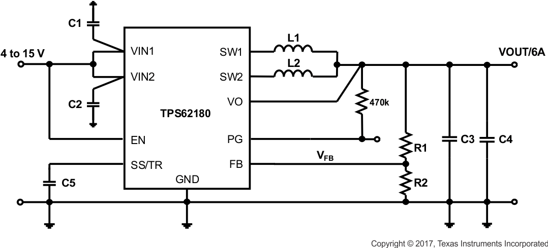 Figure 10. Typical 4-V to 15-V Input, 6A Converter
spacing
9.2.1.1 Design Requirements
The design guideline provides a component selection to operate the device within the recommended operating conditions. The component selection is given in Table 2 and gives a total solution size of about 99 mm2 with a maximum height of 2.1 mm:
Table 2. Components Used for Application Characteristics
| REFERENCE NAME | DESCRIPTION / VALUE | MANUFACTURER |
|---|---|---|
| TPS62180YZF | 2 phase step down converter, 2 x 3 mm WCSP | Texas Instruments |
| L1, L2 | Inductor XFL4020-102ME, 1 µH ±20%, 4 x 4 x 2.1 mm | Coilcraft |
| C1, C2 | Ceramic capacitor GRM21BR61E226ME44, 2 x 22 µF, 25 V, X5R, 0805 | muRata |
| C3, C4 | Ceramic capacitor GRM21BR60J476ME15, 2 x 47 µF, 6.3 V, X5R, 0805 | muRata |
| C5 | Ceramic capacitor, 3.3 nF | Standard |
| R1 | Chip resistor, value depending on VOUT | Standard |
| R2 | Chip resistor, value depending on VOUT | Standard |
| R3 | Chip resistor, 470 kΩ, 0603, 1/16 W, 1% | Standard |
9.2.1.2 Detailed Design Procedure
9.2.1.2.1 Custom Design With WEBENCH® Tools
Click here to create a custom design using the TPS62180 device with the WEBENCH® Power Designer.
- Start by entering the input voltage (VIN), output voltage (VOUT), and output current (IOUT) requirements.
- Optimize the design for key parameters such as efficiency, footprint, and cost using the optimizer dial.
- Compare the generated design with other possible solutions from Texas Instruments.
The WEBENCH Power Designer provides a customized schematic along with a list of materials with real-time pricing and component availability.
In most cases, these actions are available:
- Run electrical simulations to see important waveforms and circuit performance
- Run thermal simulations to understand board thermal performance
- Export customized schematic and layout into popular CAD formats
- Print PDF reports for the design, and share the design with colleagues
Get more information about WEBENCH tools at www.ti.com/WEBENCH.
9.2.1.2.2 Programming the Output Voltage
The output voltage of the TPS62180 is programmed using an external resistive divider. While the voltage at the FB pin is regulated to 0.8 V, the output voltage range is specified from 0.9 up to 6 V. The value of the output voltage is set by selection of the resistive divider (from VOUT to FB to AGND) from Equation 9.
spacing

spacing
The current through those resistors contributes to the light load efficiency, which makes larger resistor values beneficial. However, to get sufficient noise immunity these values should not be oversized. Using this, the resistor values are calculated by converting Equation 9 as follows:
spacing

spacing
Inserting the R2 value in Equation 11, R1 can be obtained.
spacing

spacing
Calculating for VOUT = 3.3 V gives R1 = 500 kΩ. Using standard resistor values R1 = 470 kΩ and R2 = 150 kΩ are chosen.
For applications requiring lowest current consumption, the use of fixed output voltage options is recommended. Using the TPS62182, the FB pin can be left floating, but it is recommended to connect it to AGND which decreases thermal resistance.
In case the FB pin of the adjustable output voltage version gets opened or an over voltage appears at the output, an internal clamp limits the output voltage to about 7.4 V.
9.2.1.2.3 Output Filter Selection
Since the TPS6218x is compensated internally, it is optimized for a range of external component values, which is specified below. Table 3 and Table 4 are used to simplify the output filter component selection. Checked cells represent combinations that are proven for stability by simulation and lab test. Further combinations should be checked for each individual application.
Table 3. Recommended LC Output Filter Combinations for VOUT ≥ 1.8 V(1)
| 2 x 47 µF | 4 x 47 µF | 6 x 47 µF | 8 x 47 µF | |
|---|---|---|---|---|
| 0.47 µH | ||||
| 1.0 µH | √ | √ | √ | √ |
| 1.5 µH |
Table 4. Recommended LC Output Filter Combinations for VOUT < 1.8 V(1)
| 2 x 47 µF | 4 x 47 µF | 6 x 47 µF | 8 x 47 µF | |
|---|---|---|---|---|
| 0.68 µH | ||||
| 1.0 µH | √ | √ | ||
| 1.5 µH |
For the output capacitors, a voltage rating of 6.3 V and an X5R dielectric are chosen. If space allows for higher voltage rated capacitors in larger case sizes, the dc bias effect is lowered and the effective capacitance value increases.
9.2.1.2.4 Inductor Selection
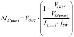
The TPS6218x is designed to work with two inductors of 1 µH nominal. They have to be selected for adequate saturation current and a low dc resistance (DCR). The minimum inductor current rating IL(min) that is needed under static load conditions is calculated using Equation 12 and Equation 13. A current imbalance of 10% at most is incorporated.
spacing

spacing
spacing
spacing
This calculation gives the minimum saturation current of the inductor needed and an additional margin of about 20% is recommended to cover dynamic overshoot due to load transients. For low profile solutions, the physical inductor size and the power losses have to be traded off. Smallest solution size (for example with chip inductors) are less efficient than bigger inductors with lower losses due to lower DCR and/or core losses. The following inductors have been tested with the TPS6218x:
Table 5. List of Inductors
| TYPE | INDUCTANCE [µH] | CURRENT RATING MIN/TYP [A] (1) | DCR MAX [mΩ] | DIMENSIONS (LxBxH) [mm] | MANUFACTURER |
|---|---|---|---|---|---|
| DFE201612E-1R0M | 1 ±20% | 4.0/4.4 | 48 | 2.0 x 1.6 x 1.2 | TOKO |
| DFE252012F-1R0M | 1 ±20% | 4.7/5.3 | 40 | 2.5 x 2.0 x 1.2 | TOKO |
| DFE252012P-1R0M | 1 ±20% | 3.8/4.5 | 42 | 2.5 x 2.0 x 1.2 | TOKO |
| PIFE32251B-1R0MS | 1 ±20% | 4.2/4.7 | 42 | 3.2 x 2.5 x 1.2 | CYNTEC |
| PIME031B-1R0MS | 1 ±20% | 4.5/5.4 | 55 | 3.7 x 3.3 x 1.2 | CYNTEC |
| PISB25201T-1R0MS | 1 ±20% | 3.6/3.9 | 62 | 2.5 x 2.0 x 1.0 | CYNTEC |
| IHLP1212AB-11 | 1 ±20% | /5.0 | 37.5 | 3.6 x 3.0 x 1.2 | VISHAY |
| IHLP1212AE-11 | 1 ±20% | /5.3 | 33 | 3.6 x 3.0 x 1.5 | VISHAY |
| XFL4015-122ME_ | 1.2±20% | /4.5 | 20.7 | 4.0 x 4.0 x 1.5 | COILCRAFT |
| XFL4020-102ME_ | 1 ±20% | /5.4 | 11.9 | 4.0 x 4.0 x 2.1 | COILCRAFT |
| TFM201610-GHM | 1 ±20% | 3.6/3.8 | 60 | 2.0 x 1.6 x 1.0 | TDK |
| TFM252010-GHM | 1 ±20% | 3.5/4.0 | 56 | 2.5 x 2.0 x 1.0 | TDK |
The TPS6218x is not designed to operate with only one inductor.
9.2.1.2.5 Output Capacitor Selection
The TPS6218x provides a wide output voltage range of 0.9 V to 6 V. While stability is a critical criteria for the output filter selection, the output capacitor value also determines transient response behavior, ripple and accuracy of VOUT. Table 6 gives recommendations to achieve various transient design targets using 1-µH inductors and small sized output capacitors (see Table 2).
Table 6. Recommended Output Capacitor Values
| OUTPUT VOLTAGE [V] | LOAD STEP [A] | (NOMINAL) CAPACITOR VALUE(3) | TYPICAL TRANSIENT RESPONSE ACCURACY | |
|---|---|---|---|---|
| ±mV | ±% | |||
| 0.9(2) | 2-6-2(1) | 4 x 47 µF | 90 | 10 |
| 6 x 47 µF | 70 | 8 | ||
| 1.8 | 2-6-2(1) | 2 x 47 µF | 150 | 8 |
| 4 x 47 µF | 120 | 7 | ||
| 8 x 47 µF | 90 | 5 | ||
| 3.3 | 2-6-2(1) | 2 x 47 µF | 170 | 5 |
| 4 x 47 µF | 135 | 4 | ||
| 8 x 47 µF | 100 | 3 | ||
spacing
The architecture of the TPS6218x allows the use of tiny ceramic output capacitors with low equivalent series resistance (ESR). These capacitors provide low output voltage ripple and are recommended. To keep its low resistance up to high frequencies and to get narrow capacitance variation with temperature, it is recommended to use X7R or X5R dielectrics. Using even higher values than demanded for stability and transient response has further advantages like smaller voltage ripple and tighter dc output accuracy in Power Save Mode.
9.2.1.2.6 Input Capacitor Selection
The input current of a buck converter is pulsating. Therefore, a low ESR input capacitor is required to prevent large voltage transients and provide peak currents. The recommended value for most applications is 2 x 22 µF, split between the VIN1 and VIN2 inputs and placed as close as possible to these pins and PGND pins. If additional capacitance is needed, it can be added as bulk capacitance. To ensure proper operation, the effective capacitance at the VIN pins must not fall below 2 x 2 µF (close) + 10 µF bulk (effective capacitances).
Low ESR multilayer ceramic capacitors are recommended for best filtering. Increasing with input voltage, the dc bias effect reduces the nominal capacitance value significantly. To decrease input ripple current further, larger values of input capacitors can be used.
9.2.1.2.7 Soft Start Capacitor Selection
The TPS6218x provides a user programmable soft start time. A constant current source of 5 µA, internally connected to the SS/TR pin, allows control of the startup slope by connecting a capacitor to this pin. The current source charges the capacitor and the soft start time is given by:
spacing

spacing
where CSS is the soft-start capacitance required at the SS/TR pin and tss is the resulting soft-start ramp time.
spacing
The SS/TR pin should not be left floating and a minimum capacitance of 220 pF is recommended. Using Equation 14, and inserting tSS = 750 µs, a value of 3 nF is calculated. 3.3 nF is chosen as a standard value for this example.
9.2.1.3 Application Performance Curves
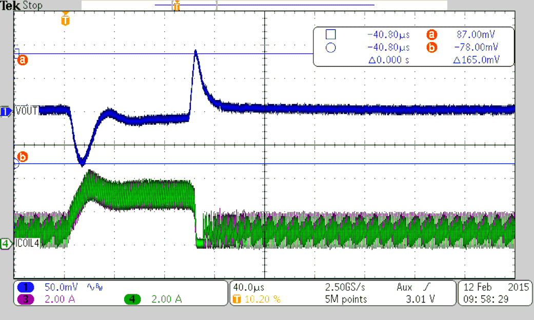
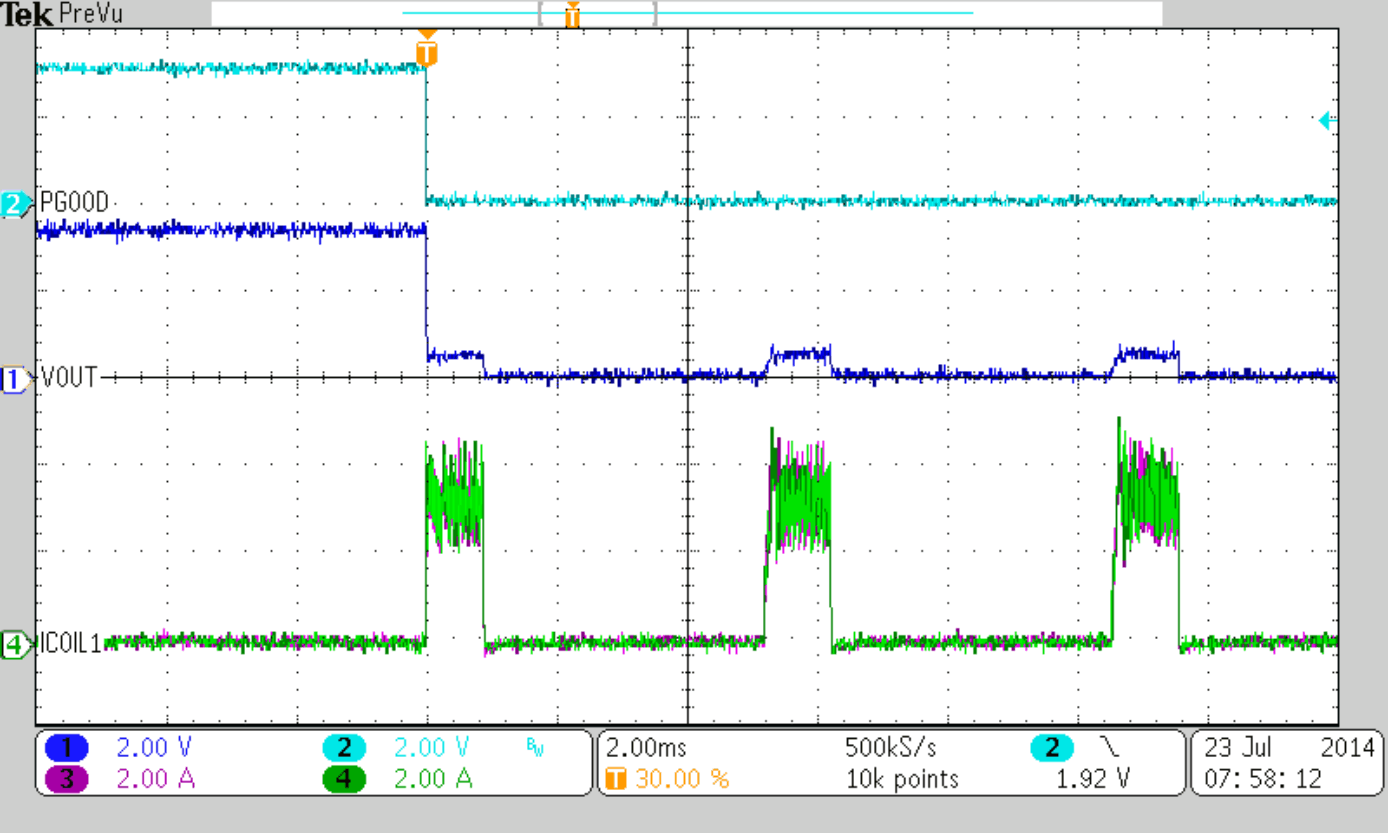
VIN = 12 V, VOUT = 3.3 V, TA = 25°C, (unless otherwise noted)
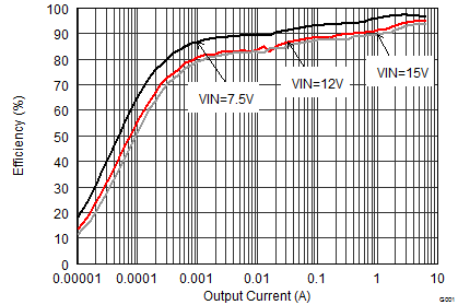
| VOUT = 6 V |

| VOUT = 3.3 V |
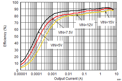
| VOUT = 1.8 V |
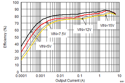
| VOUT = 0.9 V | ||
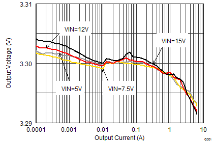
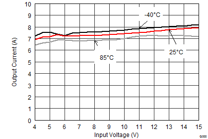
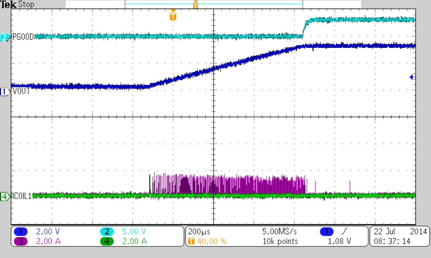
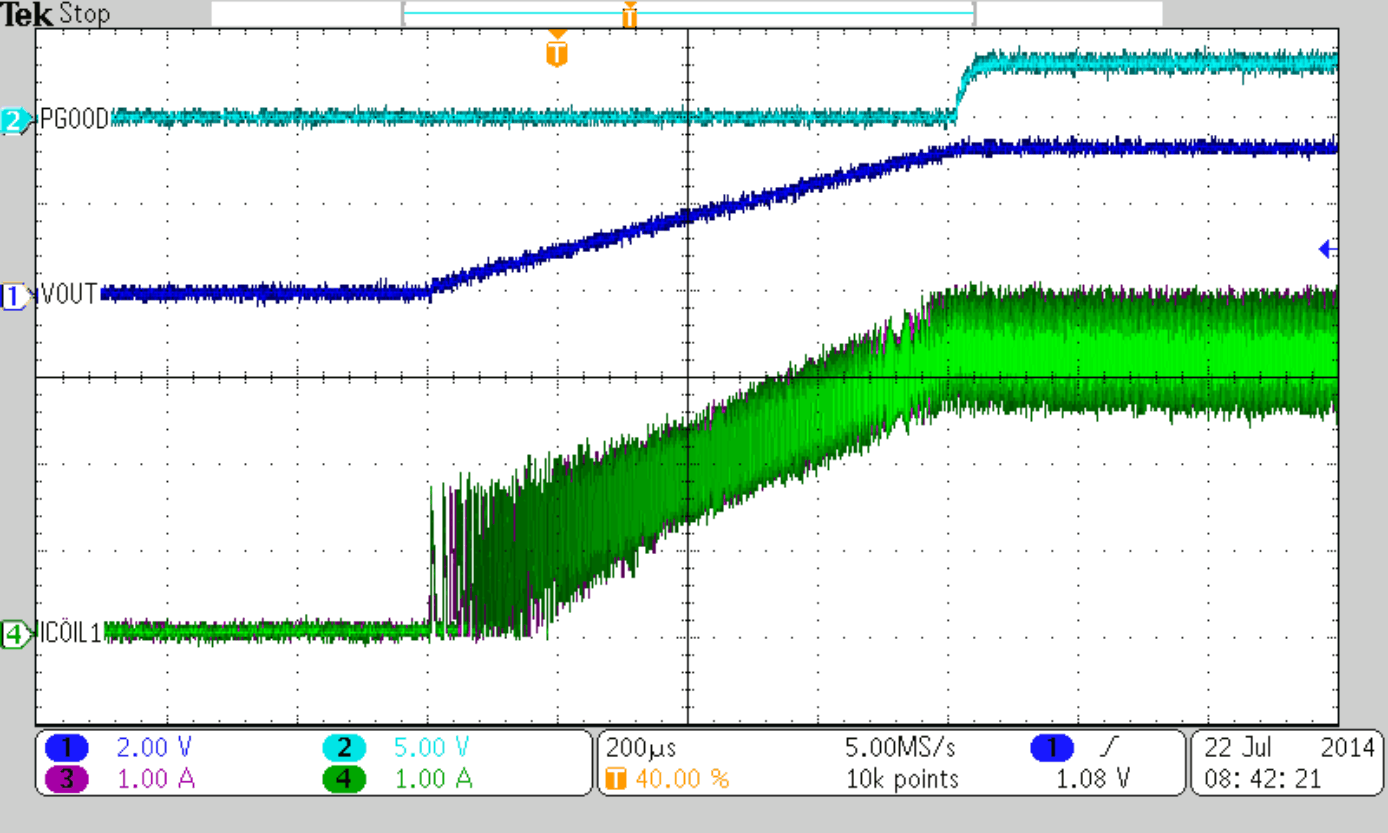
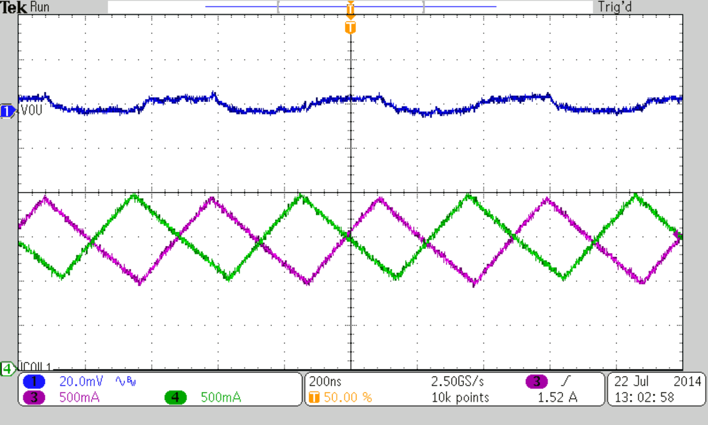
| IOUT = 3 A | ||
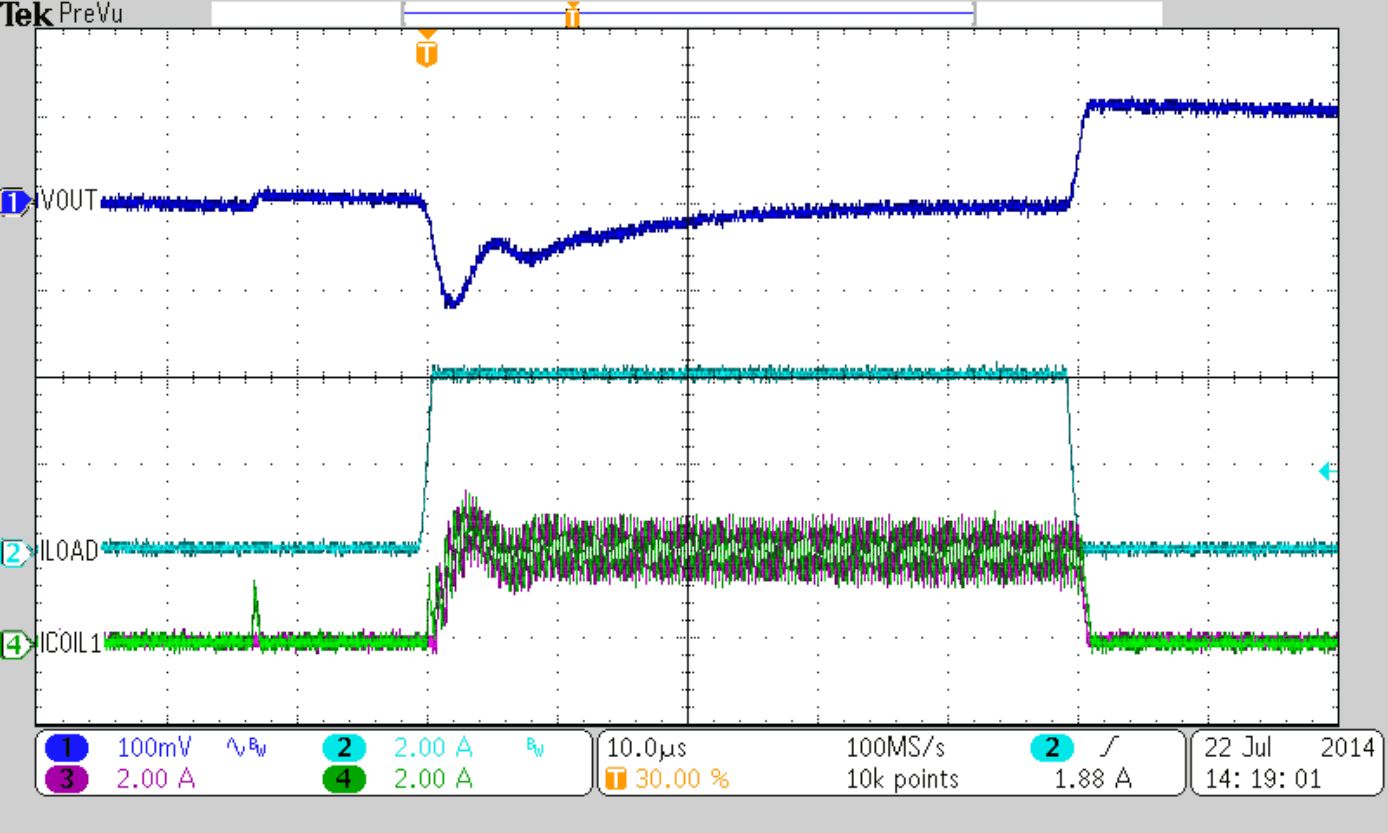
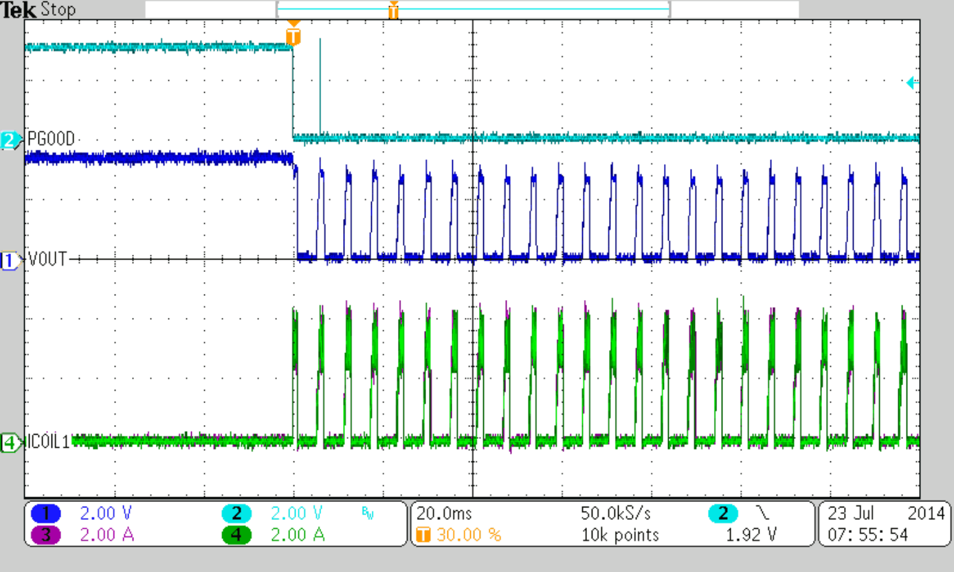
| RLOAD = 0.33 Ω | ||
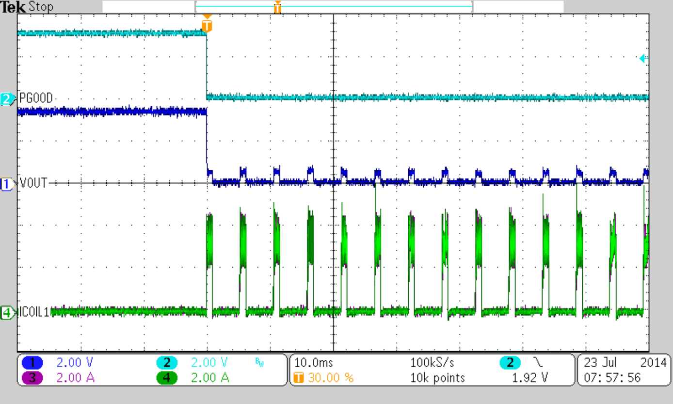
| VOUT = 6 V |
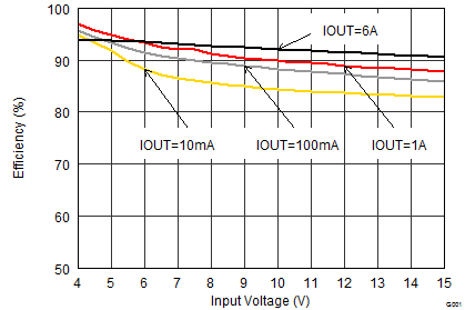
| VOUT = 3.3 V |
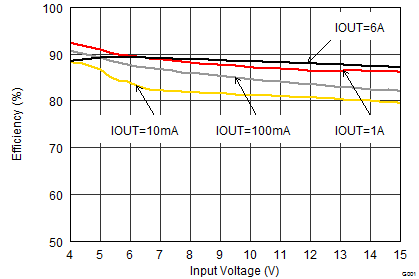
| VOUT = 1.8 V |
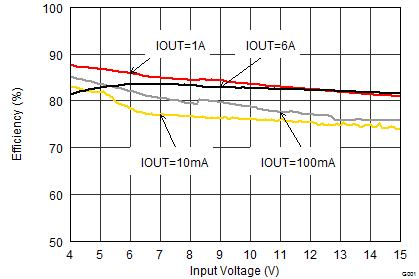
| VOUT = 0.9 V | ||
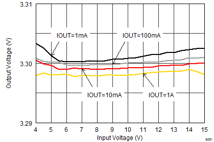
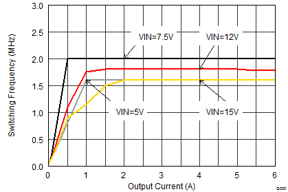
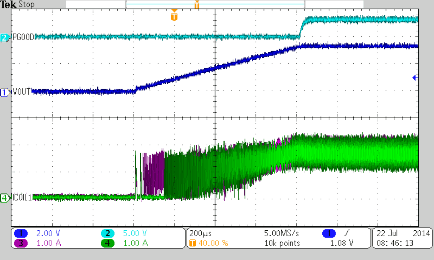
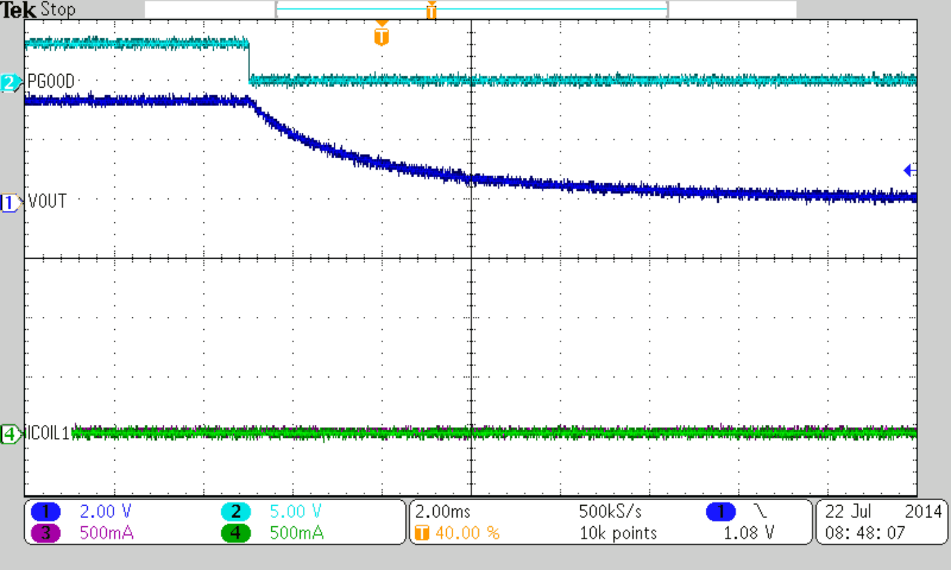
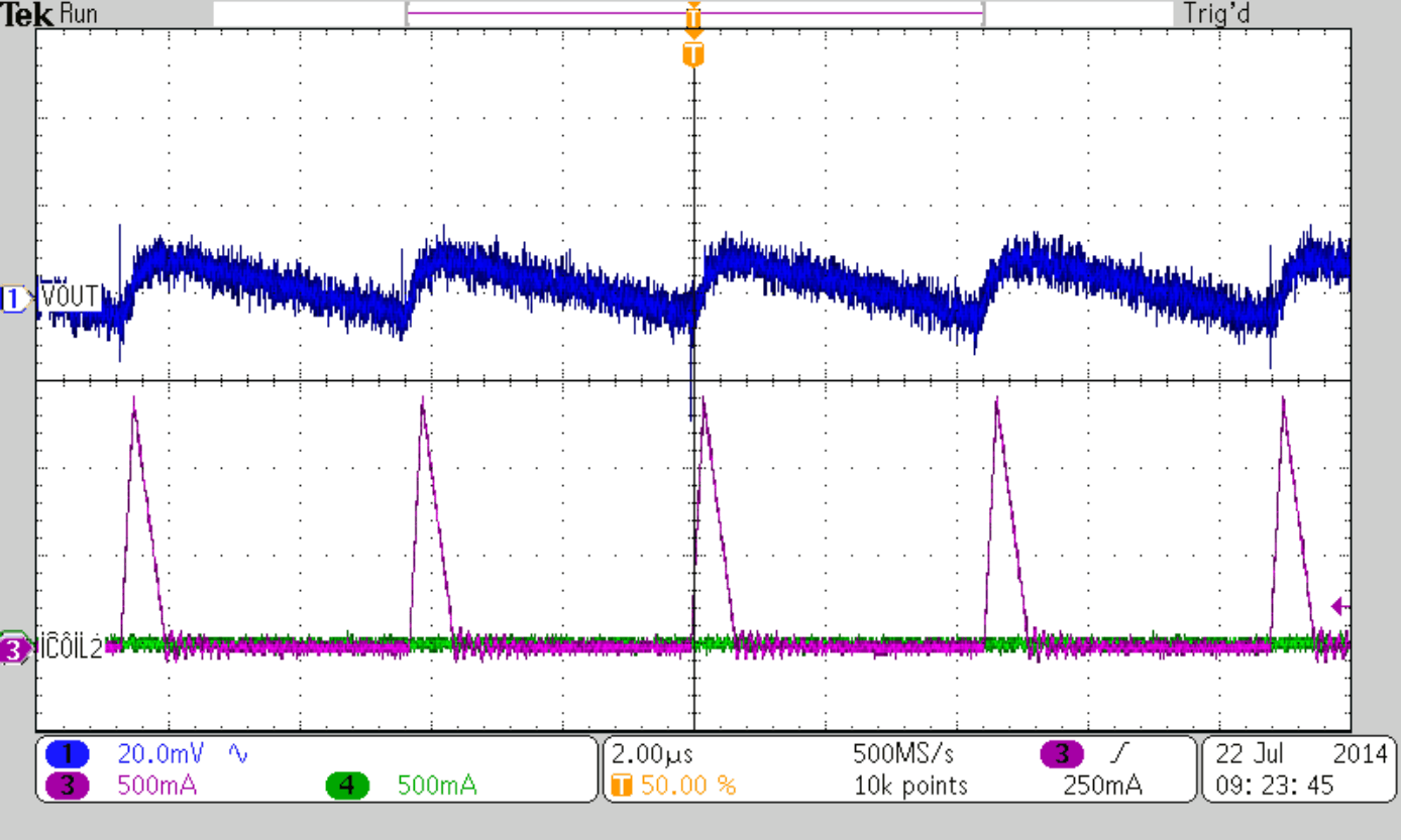
| IOUT = 100 mA | ||
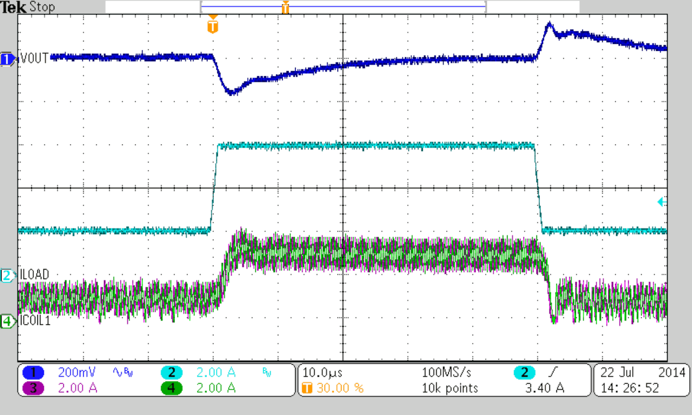
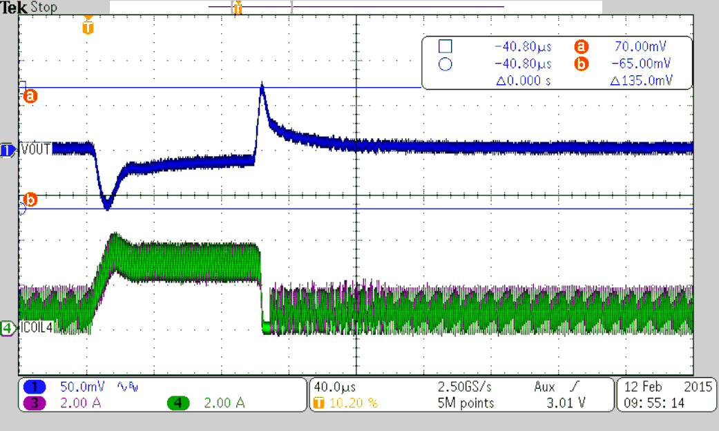
| VOUT = 1.8 V | COUT = 6x47 µF | additional CFF = 82 pF |
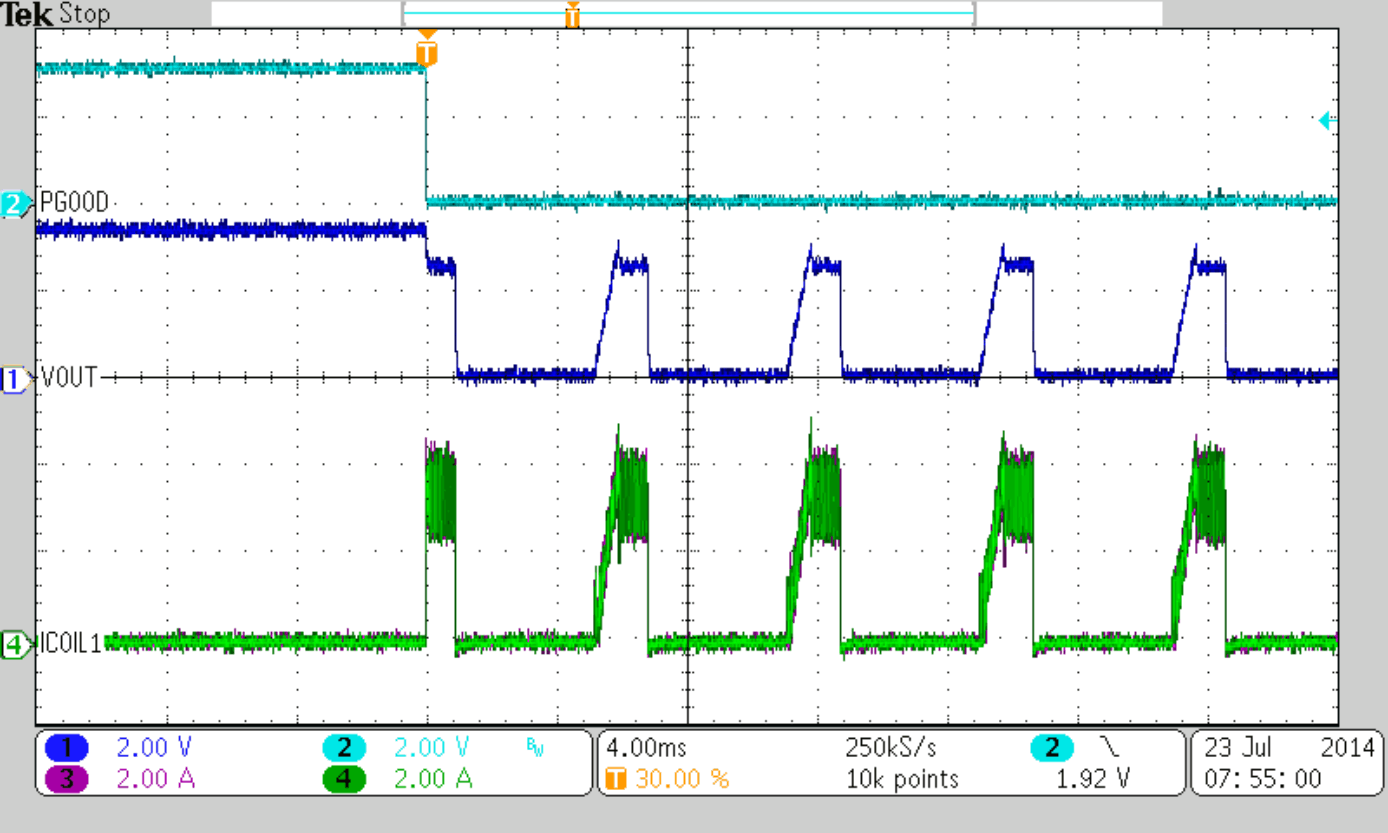
| RLOAD = 0.33 Ω | ||
space
9.2.2 TPS62180 Low Profile Solution
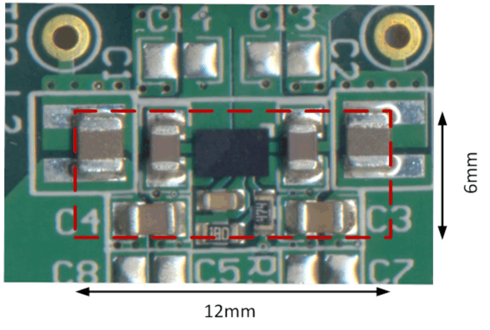
This design example is based on Figure 10 again, providing a very small (see Figure 38) and low profile solution, using low profile inductors.
9.2.2.1 Design Requirements
The input parameters used for this design are given in Table 7 and give a total solution size of about 72mm2, using inductors with a maximum height of 1.2 mm:
Table 7. Components Used for Application Characteristics
| REFERENCE NAME | DESCRIPTION / VALUE | MANUFACTURER |
|---|---|---|
| TPS62180YZF | 2 phase step down converter, 2 x 3 mm WCSP | Texas Instruments |
| L1, L2 | Inductor DFE252012P, 1 µH ±20%, 2.5 x 2 x 1.2 mm | Toko |
| CIN | Ceramic capacitor GRM21BR61E226ME44, 2 x 22 µF, 25 V, X5R, 0805 | muRata |
| COUT | Ceramic capacitor GRM21BR60J476ME15, 2 x 47 µF, 6.3 V, X5R, 0805 | muRata |
| CSS | Ceramic capacitor, 10 nF | Standard |
| R1 | Chip resistor, value depending on VOUT | Standard |
| R2 | Chip resistor, value depending on VOUT | Standard |
| R3 | Chip resistor, 470 kΩ, 0603, 1/16 W, 1% | Standard |
space
9.2.2.2 Detailed Design Procedure
As opposed to the previous example, the solution size, including height, is limited and the soft start time is longer. This is achieved by using smaller inductors, as well as using a different soft start capacitor.
9.2.2.2.1 Inductor
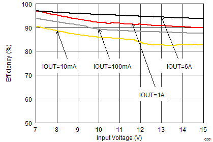
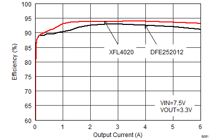
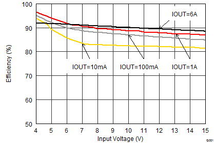
Using Table 5, the 1-µH DFE252012P is chosen with dimensions of 2.5 x 2.0 x 1.2 mm. The larger DCR of 42 mΩ maximum causes some efficiency drop (see comparison below).
space
9.2.2.2.2 Input and Output Capacitors
Since electrical design parameters are unchanged, the same values as chosen in the previous example are used for these capacitors.
9.2.2.2.3 Soft Start Capacitor
Using Equation 14 again, and inserting tSS = 2.5 ms gives a capacitance of 10 nF, which is chosen.
9.2.2.2.4 Using the Accurate EN Threshold
The TPS6218x provides a very accurate EN threshold voltage. This can be used to switch on the device according to a VIN or another voltage level by using a resistive divider as shown below.
space
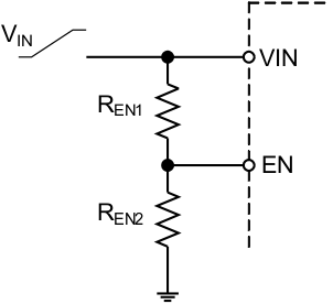 Figure 40. Resistive Divider for Controlled EN Threshold
space
The values of REN1 and REN2, needed to set EN = High at a specific VIN can be calculated according to Kirchhoff's laws, shown in Equation 15 and used in the following example:
space

space
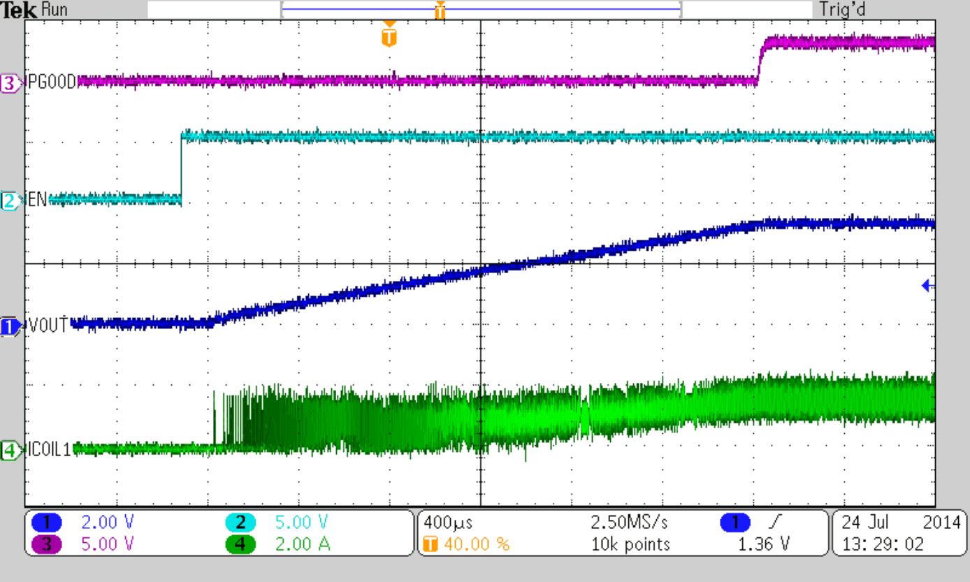
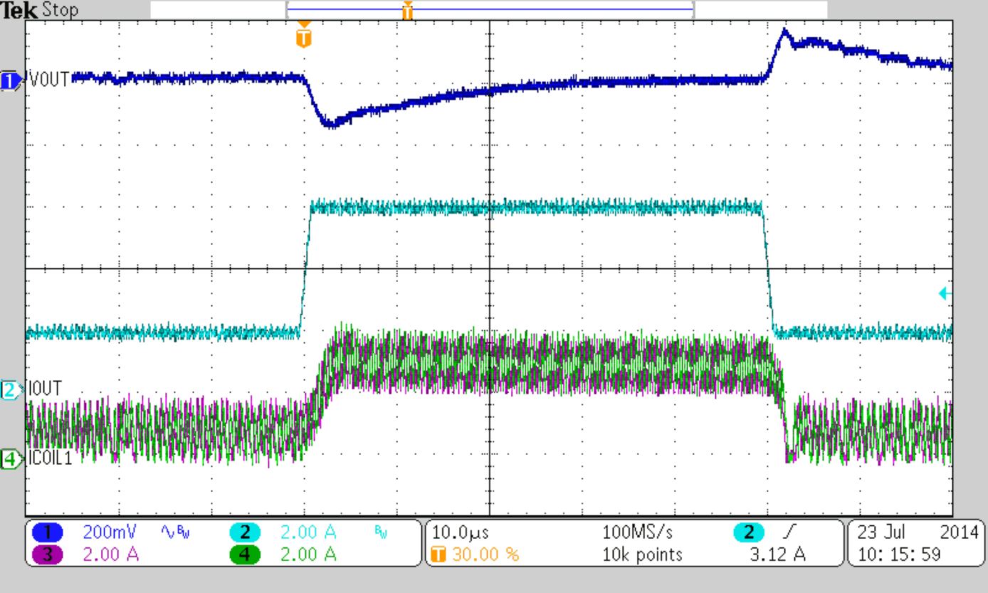
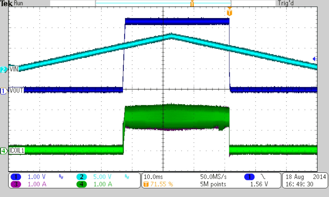
For a typical 8-V input rail, the device turn on target value is set to 5.5 V. The current through the resistive divider is set to 10 µA, which indicates a total resistance of about 800 kΩ. Appropriate standard resistor values, fitting Equation 15, are REN1 = 680 kΩ and REN2 = 150 kΩ. As a result, the device switches on, when VIN has reached 5.5 V and the current through the divider is 9.6 µA. The device switches off at a threshold of 0.9 V. Using Equation 15 again, this case gives a level of VIN = 5.0 V.
Figure 47 to Figure 50 show thresholds and appropriate device behavior with a startup time of about 800 µs.
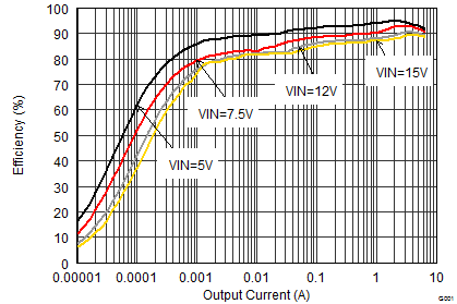
9.2.2.3 Application Performance Curves
VIN = 12 V, VOUT = 3.3 V, TA = 25°C, (unless otherwise noted)
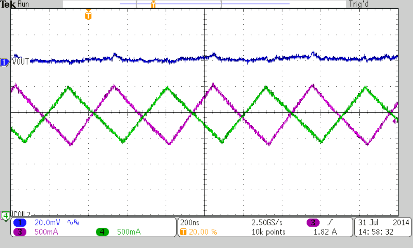
| VIN = 8 V, IOUT = 4 A |
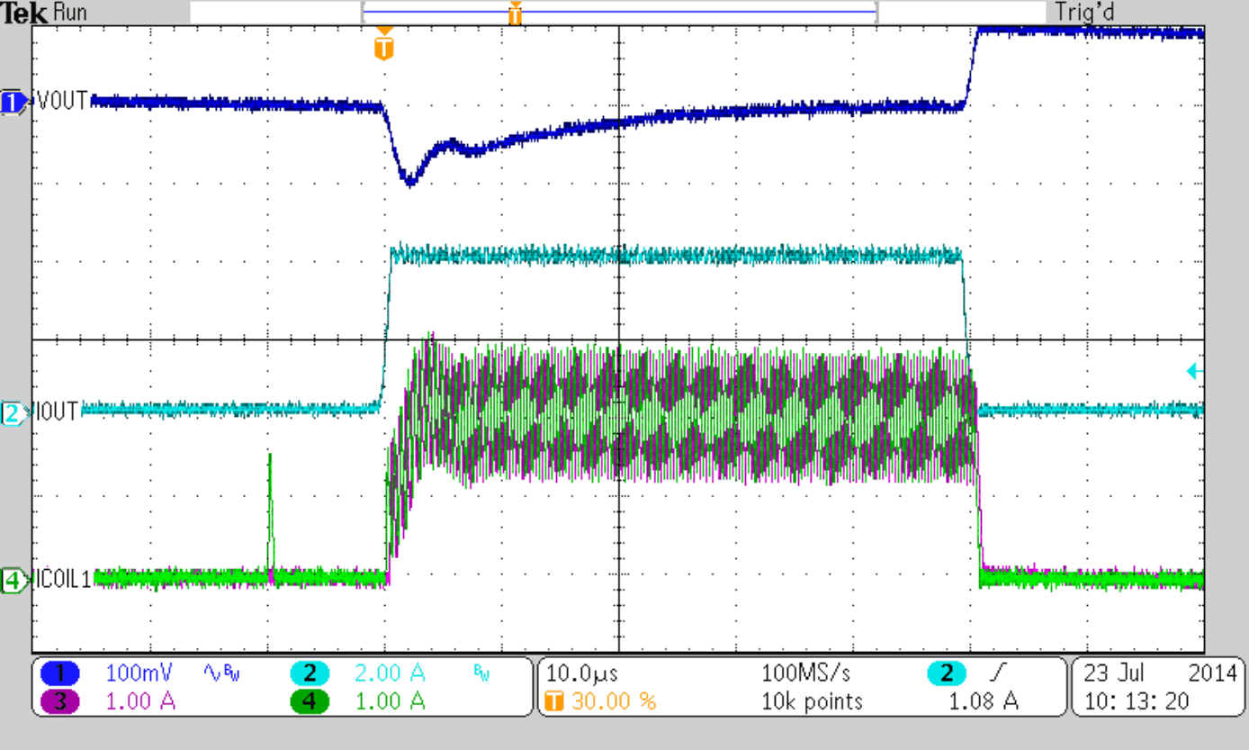
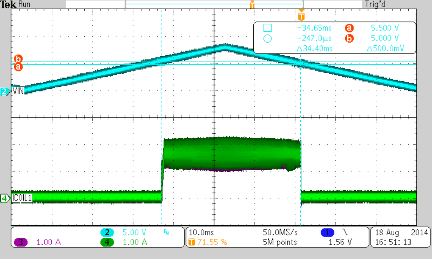
| VIN = 5.5 V (Rising), VIN = 5.0 V (Falling) | ||
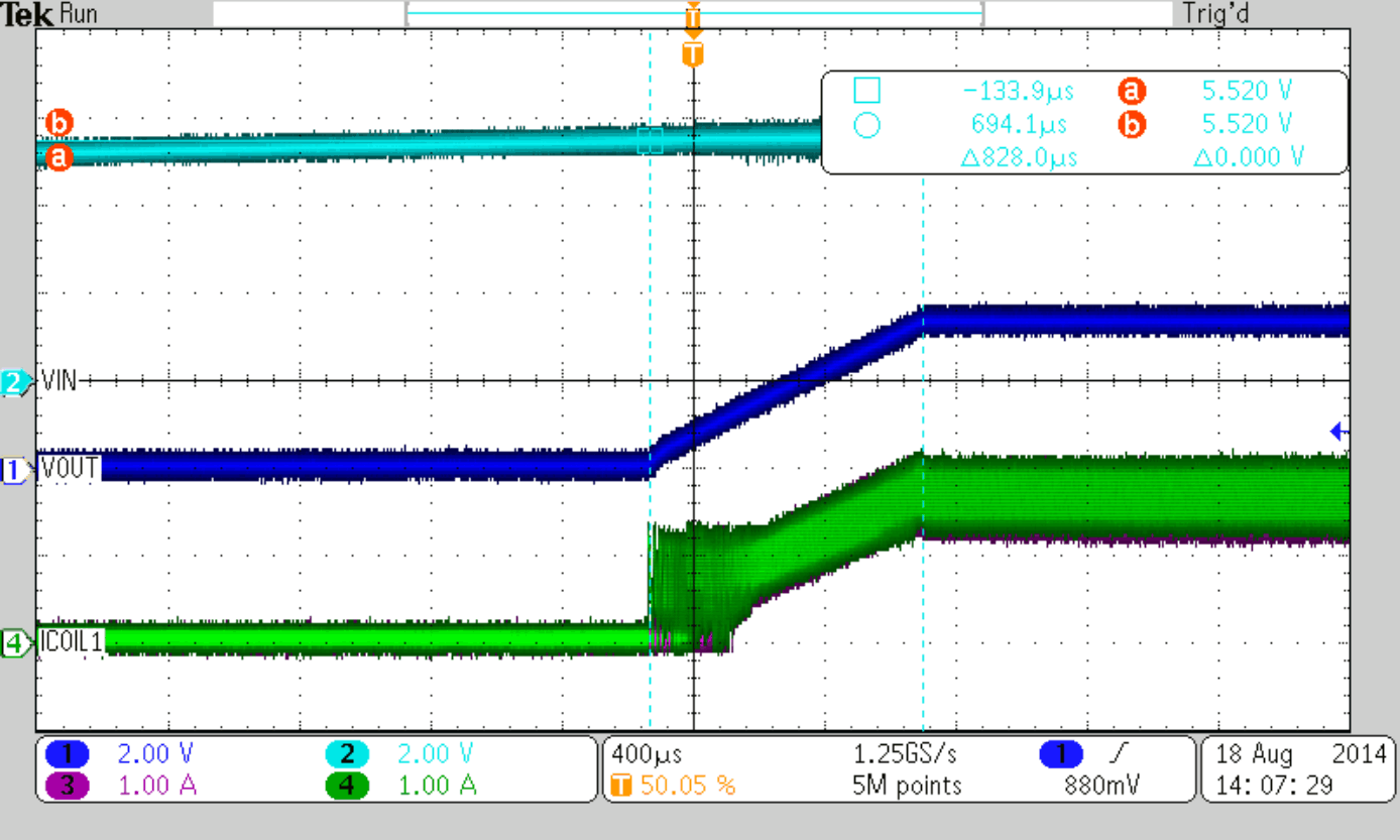
| VIN = 5.5 V (Rising) | ||
| CSS = 10 nF |
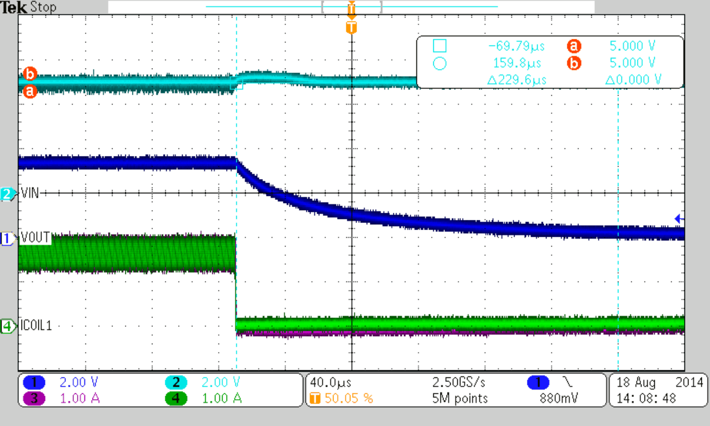
| VIN = 5.0 V (Falling) | ||
9.3 TPS62180 Output Voltage Application Examples
This section provides typical schematics for commonly used output voltage values.
9.3.1 Application Schematic Examples
space
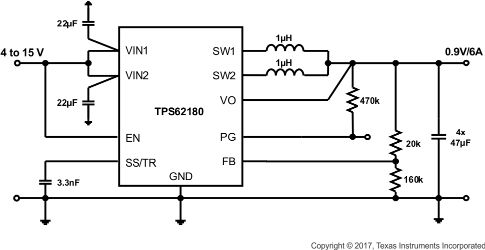 Figure 51. 0.9-V/6-A Power Supply
space
 Figure 52. 1.8-V/6-A Power Supply
space
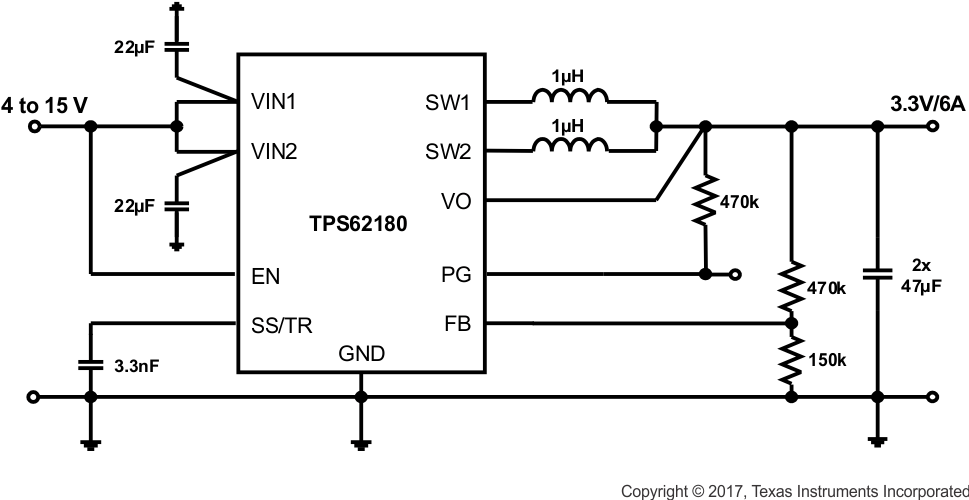 Figure 53. 3.3-V/6-A Power Supply
space
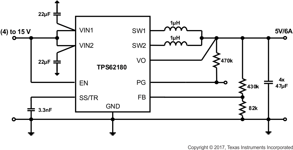 Figure 54. 5-V/6-A Power Supply
9.3.2 Design Requirements
Based on Figure 10, the schematics shown in Figure 51 through Figure 54 show different output voltage divider values to get different VOUT. Another design target is to have about 5-µA current through the divider.
9.3.3 External Component Selection
The values for the voltage divider are derived using the procedure given in Programming the Output Voltage. While Equation 10 and Equation 11 are used to calculate R2 and R1, the values are aligned with standard resistor values.
