-
TPS62231x-Q1 3-MHz Ultra-Small Step-Down Converter in 1 × 1.5 SON Package SLVSB63A December 2011 – March 2016 TPS62231-Q1 , TPS622314-Q1
PRODUCTION DATA.
-
TPS62231x-Q1 3-MHz Ultra-Small Step-Down Converter in 1 × 1.5 SON Package
- 1 Features
- 2 Applications
- 3 Description
- 4 Revision History
- 5 pPin Configuration and Functions
- 6 Specifications
- 7 Detailed Description
- 8 Application and Implementation
- 9 Power Supply Recommendations
- 10Layout
- 11Device and Documentation Support
- 12Mechanical, Packaging, and Orderable Information
- IMPORTANT NOTICE
パッケージ・オプション
メカニカル・データ(パッケージ|ピン)
- DRY|6
サーマルパッド・メカニカル・データ
- DRY|6
発注情報
TPS62231x-Q1 3-MHz Ultra-Small Step-Down Converter in 1 × 1.5 SON Package
1 Features
- Qualified for Automotive Applications
- Up to 3.8-MHz Switch Frequency
- Up to 94% Efficiency
- Output Peak Current up to 500 mA
- Excellent AC and Transient Load Regulation
- High PSRR (up to 90 dB)
- Small External Output-Filter Components 1 μH and 4.7 μF
- VIN range from 2.05 V to 6 V
- Optimized Power Save Mode For Low Output-Ripple Voltage
- Forced PWM Mode Operation
- Typical 22-μA Quiescent Current
- 100% Duty Cycle for Lowest Dropout
- Small 1 × 1.5 × 0.6-mm3 SON Package
- 12-mm2 Minimum Solution Size
- Supports 0.6-mm Maximum Solution Height
- Soft Start With 100-μs (Typical) Start-Up Time
2 Applications
3 Description
The TPS6223x-Q1 device family is a high-frequency, synchronous step-down DC-DC converter ideal for space-optimized automotive and industrial applications. The device supports up to 500-mA output current and allows the use of tiny and low-cost chip inductors and capacitors.
With a wide input-voltage range of 2.05 V to 6 V, the device can be powered by a preregulated voltage rail or Li-Ion batteries with extended voltage range. Two different fixed-output voltage versions are available at 1.5 V and 1.8 V.
The TPS6223x-Q1 series features switch frequency up to 3.8 MHz. At medium to heavy loads, the converter operates in PWM mode and automatically enters Power Save Mode operation at light load currents to maintain high efficiency over the entire load current range.
Because of its excellent PSRR and AC load regulation performance, the device is also suitable to replace linear regulators to obtain better power conversion efficiency.
The Power Save Mode in TPS6223x-Q1 reduces the quiescent current consumption down to 22 μA during light load operation. It is optimized to achieve very low output voltage ripple even with small external component and features excellent AC load regulation.
For noise-sensitive applications, the device can be forced to PWM Mode operation over the entire load range by pulling the MODE pin high. In the shutdown mode, the current consumption is reduced to less than 1 μA. The TPS6223x-Q1 is available in a 1-mm × 1.5-mm2 6-pin SON package.
Device Information(1)
| PART NUMBER | OUTPUT VOLTAGE |
FREQUENCY |
|---|---|---|
| TPS62231-Q1 | 1.8 V | 3 MHz |
| TPS622314-Q1 | 1.5 V | 3 MHz |
- For all available packages, see the orderable addendum at the end of the data sheet.
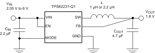
Typical Application Schematic

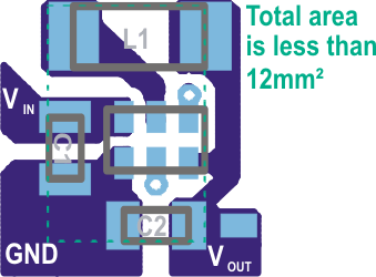
Small PCB Layout Size

4 Revision History
Changes from * Revision (December 2011) to A Revision
- Added Pin Configuration and Functions section, ESD Ratings table, Thermal Information table, Feature Description section, Device Functional Modes, Application and Implementation section, Power Supply Recommendations section, Layout section, Device and Documentation Support section, and Mechanical, Packaging, and Orderable Information sectionGo
- Changed the Applications list Go
- Deleted the Ordering Information table Go
- Deleted references to devices and voltage options that are not available as automotive gradeGo
- Added minimum and maximum recommended values for output inductance and output capacitance in the Recommended Operating Conditions table for clarityGo
- Deleted the Dissipation Ratings table and added a more detailed Thermal Information tableGo
- Deleted the Parameter Measurement Information sectionGo