SLVS651B May 2006 – December 2015 TPS62510
PRODUCTION DATA.
- 1 Features
- 2 Applications
- 3 Description
- 4 Revision History
- 5 Pin Configuration and Functions
- 6 Specifications
- 7 Detailed Description
- 8 Application and Implementation
- 9 Power Supply Recommendations
- 10Layout
- 11Device and Documentation Support
- 12Mechanical, Packaging, and Orderable Information
パッケージ・オプション
メカニカル・データ(パッケージ|ピン)
- DRC|10
サーマルパッド・メカニカル・データ
- DRC|10
発注情報
7 Detailed Description
7.1 Overview
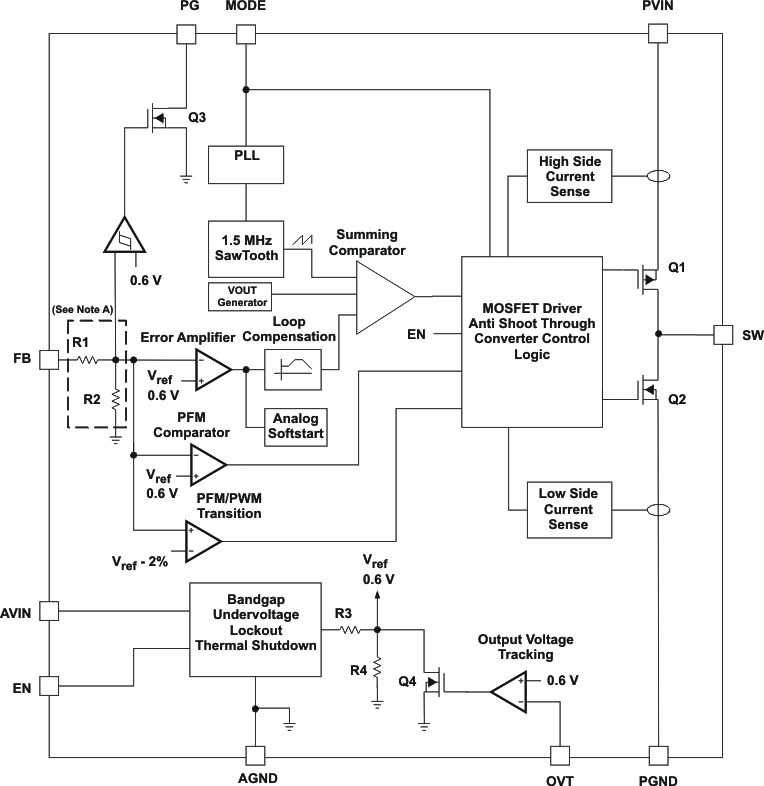
The TPS62510 has two target areas of operation. The high efficiency area is defined when the MODE pin is held low. In this condition, the converter operates at typically 1.5-MHz fixed frequency pulse width modulation (PWM) mode at moderate to heavy load currents. At light load currents, the converter automatically enters power save mode and operates with pulse frequency modulation (PFM) mode. Low noise operation is defined when the MODE pin is held high. In this condition, the converter is forced into fixed frequency PWM mode and runs at 1.5 MHz. The converter is capable of delivering 1.5-A output current.
The TPS62510 can also be synchronized to an external clock in the frequency range between 1.15 MHz and 2.25 MHz. Synchronization is aligned with the falling edge of the incoming clock signal. This allows simple synchronization of two step-down converters running 180° out of phase reducing overall input RMS current.
During PWM operation, the converters use a unique fast response voltage mode control scheme with input voltage feed-forward to achieve good line, and load regulation allowing the use of small ceramic input and output capacitors. At the beginning of each clock cycle initiated by the clock signal, the P-channel MOSFET switch is turned on, and the inductor current ramps up until the comparator trips and the control logic turns off the switch. The current limit comparator also turns off the switch if the current limit of the P-channel switch is exceeded. After the adaptive dead time, which is used to prevent shoot through current, the N-channel MOSFET rectifier is turned on, and the inductor current ramps down. The next cycle is initiated by the clock signal turning off the N-channel rectifier, and turning on the P-channel switch.
7.2 Functional Block Diagram
7.3 Feature Description
7.3.1 Output Voltage Tracking (OVT)
In applications where a processor or FPGA is powered, it is important that the I/O voltage and core voltage start-up in a controlled way to avoid possible processor and FPGA latch-up. To implement this, the TPS62510 has an output voltage tracking feature where the internal reference voltage for the error amplifier follows the voltage applied to OVT, until OVT reaches Vref. Vref is the nominal internal reference voltage, typically 0.6 V. Figure 7 shows a typical application where an external voltage (V1) is applied to OVT pin using a resistor divider.
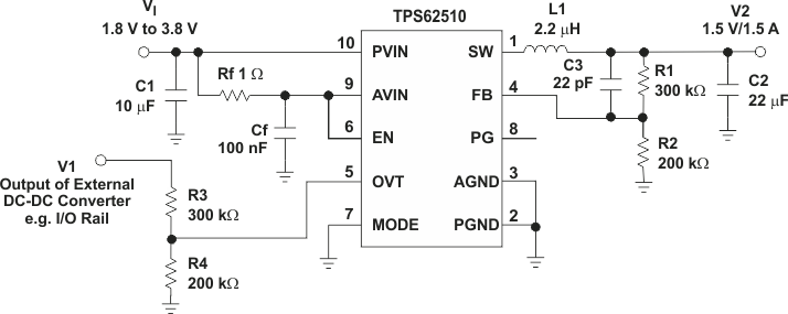 Figure 7. Output Voltage Tracking, V2 Tracks V1
In this application, the output voltage (V2) of the TPS62510 tracks the voltage (V1) as long as the OVT voltage is smaller than the internal device reference voltage, Vref = 0.6 V. Depending on the resistor divider (R3, R4), the tracking can be adjusted. V2 can rise faster, at the same timer, or slower than V1.
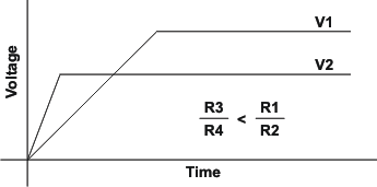 Figure 8. V2 Comes Up Before V1
Simultaneous tracking is achieved when the resistor divider (R3/R4) is equal to the resistor divider of the TPS65210.


If V2 needs to rise before V1, then R4 must be increased as shown in Figure 9.
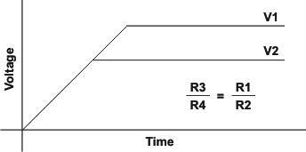 Figure 9. Simultaneous Tracking of V2 and V1
If V2 needs to rise after V1, then R4 must be decreased as shown in Figure 10.
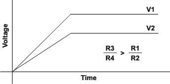 Figure 10. V2 Comes Up After V1
7.3.2 Power Good
The power good output can be used for sequencing purposes, enabling a separate regulator once the output voltage is reached, or to indicate that the output voltage is in regulation. When the device is disabled, the PG pin is pulled low by the internal open-drain output transistor. Internally, the TPS62510 compares the feedback voltage FB to the nominal reference voltage of typically 0.6 V. If the feedback voltage is more than 95% of this value then the power good output goes high impedance. If the feedback voltage is less than 90% of the reference voltage then PG pin is pulled low.
7.3.3 Undervoltage Lockout
The undervoltage lockout circuit prevents the device from malfunctioning at low input voltages. It disables the converter. The UVLO circuit monitors the AVIN pin, the falling threshold is set internally to 1.55 V with 150-mV hysteresis. Note that when the DC/DC converter is running, there is an input current at the AVIN pin, which is up to 5 mA when in PWM mode. This current must be taken into consideration if an external RC filter is used at the AVIN pin to remove switching noise from the TPS62510 internal analog circuitry supply.
7.3.4 Thermal Shutdown
As soon as the device junction temperature exceeds 160°C (typical), all switching activity ceases and both high-side and low-side power transistors are off. The device continues operation once the temperature fall to 20°C (typical) below its thermal shutdown threshold of 160°C.
7.4 Device Functional Modes
7.4.1 Soft Start
The converter has an internal soft start circuit that limits the inrush current during start-up. The soft start is realized by using a low current to control the output of the error amplifier during start-up. The soft start time is typically 750 μs to ramp the output voltage to 95% of the final target value. There is a short delay of typically 120 μs between the converter being enabled and switching activity actually starting. See the typical soft start characteristic shown in Figure 20.
7.4.2 100% Duty Cycle Low Dropout Operation
The TPS62510 converter offers a low input to output voltage difference while maintaining operation with the use of the 100% duty cycle mode. In this mode, the P-channel switch is constantly turned on. This is particularly useful in battery-powered applications to achieve longest operation time by taking full advantage of the entire battery voltage range. The minimum input voltage required to maintain DC regulation depends on the load current and output voltage, as shown in Equation 3.

where
- IOmax = Maximum load current (Note: ripple current in the inductor is zero under these conditions)
- RDS(on)max = Maximum P-channel switch RDS(on)
- RL = DC resistance of the inductor
- VOmin = Nominal output voltage minus 2% tolerance limit
7.4.3 Power Save Mode Operation (MODE)
When the MODE pin is connected to GND, the device automatically enters the power save mode when the average output current reaches the appropriate threshold. This reduces the switching frequency and minimum quiescent current, maintaining efficiency over the entire load current range. For low noise operation, the device can be forced into fixed frequency PWM mode operating at 1.5 MHz over the entire load current range. This is done by pulling the MODE pin high.
Many applications require a low output ripple voltage during power save mode. This is accomplished by a single threshold PFM comparator which allows control of the output voltage ripple in power save mode. The larger the output capacitor value, the smaller the output voltage ripple (see Figure 19). During power save mode, the device monitors the output voltage with the PFM comparator. As soon as the output voltage falls below the nominal output voltage, the device starts switching for a minimum of 1 μs (typical), or until the output voltage is above the nominal output voltage.
7.4.4 Power Save Mode Transition Thresholds
To achieve an accurate transition into and out of power save mode, the device monitors the average inductor current which is equal to the average output current. The device enters power save mode when the average output current is ≤ I(PFM enter) as calculated in Equation 4.

The device leaves the power save mode when the output current is ≥ I(PFM enter).

To minimize any delay times during a load transient, the device enters PWM mode when the output voltage is 2% below the nominal value, and the PFM/PWM transition comparator trips.
7.4.5 Short-Circuit Protection
The TPS62510 monitors the forward current through both the high-side and low-side power devices. This enables the converter to limit the short-circuit current, which helps to protect the device and other circuits connected to its output.