SLVS651B May 2006 – December 2015 TPS62510
PRODUCTION DATA.
- 1 Features
- 2 Applications
- 3 Description
- 4 Revision History
- 5 Pin Configuration and Functions
- 6 Specifications
- 7 Detailed Description
- 8 Application and Implementation
- 9 Power Supply Recommendations
- 10Layout
- 11Device and Documentation Support
- 12Mechanical, Packaging, and Orderable Information
パッケージ・オプション
メカニカル・データ(パッケージ|ピン)
- DRC|10
サーマルパッド・メカニカル・データ
- DRC|10
発注情報
10 Layout
10.1 Layout Guidelines
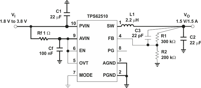
- Place and route the power components first (C1, L1, C2).
- The input capacitor (C1) must be placed as close as possible from PVIN to PGND.
- The inductor must be placed as close as possible to the switch pin.
- All ground connections (shown in bold) must be on a common ground plane or form a star ground.
- Analog ground (AGND) and power ground (PGND), as well as the exposed thermal pad, must be tight together.
- The feedback network (R1, C3, R2) must be routed away from the inductor (L1) and should be grounded to the exposed thermal pad.
- The feedback network must sense and regulate the output voltage across the output capacitor to minimize load regulation.
 Figure 22. Layout Guidelines
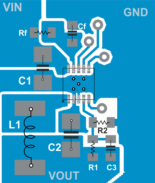
10.2 Layout Example
 Figure 23. Recommended Layout