SLVSAC5 April 2014 TPS62684
PRODUCTION DATA.
- 1 Features
- 2 Applications
- 3 Description
- 4 Revision History
- 5 Device Comparison Table
- 6 Terminal Configuration and Functions
- 7 Specifications
- 8 Parameter Measurement Information
- 9 Detailed Description
- 10Applications and Implementation
- 11Power Supply Recommendations
- 12Layout
- 13Device and Documentation Support
- 14Mechanical, Packaging, and Orderable Information
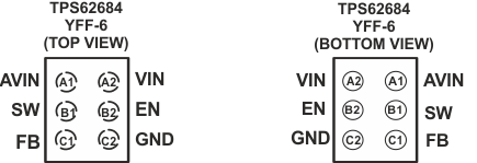
6 Terminal Configuration and Functions
6-Terminal YFF

Terminal Functions
| TERMINAL | I/O | DESCRIPTION | |
|---|---|---|---|
| NAME | NO. | ||
| FB | C1 | I | Output feedback sense input. Connect FB to the converter’s output. |
| VIN | A2 | I | Power supply input. Make sure the decoupling capacitor is connected as close as possible between terminal VIN (A2) and GND (C2). |
| AVIN | A1 | I | Bias supply input voltage pin. This pin must be connected to VIN (A2). |
| SW | B1 | I/O | This is the switch pin of the converter and is connected to the drain of the internal Power MOSFETs. |
| EN | B2 | I | This is the enable pin of the device. Connecting this pin low forces the device into shutdown mode. Pulling this pin high enables the device. This pin must not be left floating and must be terminated. When EN is pulled low, the output capacitor is actively discharged by internal circuitry. |
| GND | C2 | - | Ground pin |