JAJSLJ0B June 2015 – March 2021 TPS62746
PRODUCTION DATA
- 1 特長
- 2 アプリケーション
- 3 概要
- 4 Revision History
- 5 Device Comparison Table
- 6 Pin Configuration and Functions
- 7 Specifications
- 8 Detailed Description
- 9 Application and Implementation
- 10Power Supply Recommendations
- 11Layout
- 12Device and Documentation Support
- 13Mechanical, Packaging, and Orderable Information
6 Pin Configuration and Functions
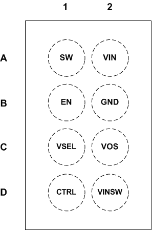
 Figure 6-1 YFP Package8-Pin DSBGATop View
Table 6-1 Pin Functions
| PIN | I/O | DESCRIPTION | |
|---|---|---|---|
| NAME | NO | ||
| VIN | A2 | PWR | VIN power supply pin. Connect the input capacitor close to this pin for best noise and voltage spike suppression. A ceramic capacitor of 4.7 µF is required. |
| SW | A1 | OUT | The switch pin is connected to the internal MOSFET switches. Connect the inductor to this terminal. |
| GND | B2 | PWR | GND supply pin. Connect this pin close to the GND terminal of the input and output capacitor. |
| VOS | C2 | IN | Feedback pin for the internal feedback divider network and regulation loop. Discharges VOUT when converter is disabled. Connect this pin directly to the output capacitor with a short trace. |
| VSEL | C1 | IN | Output voltage selection pin. See for VOUT selection. This pin must be terminated. The pin can be dynamically changed during operation. |
| EN | B1 | IN | High level enables the devices, low level turns the device off. The pin must be terminated. |
| CTRL | D1 | IN | This pin controls the input voltage switch between VIN and VINSW. With CTRL = low, the output VINSW is disabled. The pin has an internal 2 MΩ termination to GND. |
| VINSW | D2 | OUT | Output terminal of the input voltage switch. With CTRL = high, the internal switch connects the VINSW pin to the VIN pin. If not used, leave the pin open. |
Table 6-2 Output Voltage Setting
TPS62736
| DEVICE | VOUT | VSEL |
|---|---|---|
| TPS62736 | 1.2 | 0 |
| 1.8 | 1 |