SLVSES3A February 2021 – March 2021 TPS62903
PRODUCTION DATA
- 1 Features
- 2 Applications
- 3 Description
- 4 Revision History
- 5 Pin Configuration and Functions
- 6 Specifications
-
7 Detailed Description
- 7.1 Overview
- 7.2 Functional Block Diagram
- 7.3
Feature Description
- 7.3.1 Mode Selection and Device Configuration MODE/S-CONF
- 7.3.2 Adjustable VO Operation (External Voltage Divider)
- 7.3.3 Setable VO Operation (VSET and Internal Voltage Divider)
- 7.3.4 Soft Start / Tracking (SS/TR)
- 7.3.5 Smart Enable with Precise Threshold
- 7.3.6 Power Good (PG)
- 7.3.7 Undervoltage Lockout (UVLO)
- 7.3.8 Current Limit And Short Circuit Protection
- 7.3.9 Thermal Shutdown
- 7.4 Device Functional Modes
-
8 Application and Implementation
- 8.1 Application Information
- 8.2
Typical Application with Adjustable Output Voltage
- 8.2.1 Design Requirements
- 8.2.2 Detailed Design Procedure
- 8.2.3 Application Curves
- 8.2.4 Typical Application with Setable VO using VSET
- 8.3 System Examples
- 9 Power Supply Recommendations
- 10Layout
- 11Device and Documentation Support
- 12Mechanical, Packaging, and Orderable Information
3 Description
The TPS62903 is a highly-efficient, small, and flexible synchronous step-down DC-DC converter that is easy to use. A selectable switching frequency of 2.5 MHz or 1.0 MHz allows the use of small inductors and provides fast transient response. The device supports high VOUT accuracy of ± 1% with the DCS-Control topology. The wide input voltage range of 3 V to 17 V supports a variety of nominal inputs, like 12-V supply rails, single-cell or multi-cell Li-Ion, and 5-V or 3.3-V rails.
The TPS62903 can automatically enter power save mode (if auto PFM/PWM is selected) at light loads to maintain high efficiency. Additionally, to provide high efficiency at very small loads, the device has a low typical quiescent current of 4 µA. AEE, if enabled, provides high efficiency across VIN, VOUT, and load current. The device includes a MODE/Smart-CONF input to set the internal/external divider, switching frequency, output voltage discharge, and automatic power save mode or forced PWM operation.
The device is available in small 9-pin VQFN package measuring 1.50 mm × 2.00 mm with 0.5-mm pitch.
| PART NUMBER | PACKAGE(1) | BODY SIZE (NOM) |
|---|---|---|
| TPS62903 | VQFN-HR | 1.50 mm × 2.00 mm |
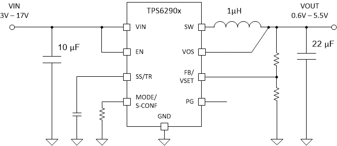
 Simplified Schematic
 Efficiency Versus Output Current (1.2-VO at 2.5 MHz-1 μH, Auto
PFM/PWM)