JAJSM97D June 2021 – August 2022 TPS62932 , TPS62933 , TPS62933F , TPS62933O , TPS62933P
PRODUCTION DATA
- 1 特長
- 2 アプリケーション
- 3 概要
- 4 Revision History
- 5 概要 (続き)
- 6 Device Comparison Table
- 7 Pin Configuration and Functions
- 8 Specifications
-
9 Detailed Description
- 9.1 Overview
- 9.2 Functional Block Diagram
- 9.3
Feature Description
- 9.3.1 Fixed Frequency Peak Current Mode
- 9.3.2 Pulse Frequency Modulation
- 9.3.3 Voltage Reference
- 9.3.4 Output Voltage Setting
- 9.3.5 Switching Frequency Selection
- 9.3.6 Enable and Adjusting Undervoltage Lockout
- 9.3.7 External Soft Start and Prebiased Soft Start
- 9.3.8 Power Good
- 9.3.9 Minimum On Time, Minimum Off Time, and Frequency Foldback
- 9.3.10 Frequency Spread Spectrum
- 9.3.11 Overvoltage Protection
- 9.3.12 Overcurrent and Undervoltage Protection
- 9.3.13 Thermal Shutdown
- 9.4 Device Functional Modes
-
10Application and Implementation
- 10.1 Application Information
- 10.2
Typical Application
- 10.2.1 Design Requirements
- 10.2.2
Detailed Design Procedure
- 10.2.2.1 Custom Design With WEBENCH® Tools
- 10.2.2.2 Output Voltage Resistors Selection
- 10.2.2.3 Choosing Switching Frequency
- 10.2.2.4 Soft-Start Capacitor Selection
- 10.2.2.5 Bootstrap Capacitor Selection
- 10.2.2.6 Undervoltage Lockout Setpoint
- 10.2.2.7 Output Inductor Selection
- 10.2.2.8 Output Capacitor Selection
- 10.2.2.9 Input Capacitor Selection
- 10.2.2.10 Feedforward Capacitor CFF Selection
- 10.2.2.11 Maximum Ambient Temperature
- 10.2.3 Application Curves
- 10.3 What to Do and What Not to Do
- 11Power Supply Recommendations
- 12Layout
- 13Device and Documentation Support
- 14Mechanical, Packaging, and Orderable Information
10.2.3 Application Curves
VIN = 24 V, VOUT = 5 V, L1= 6.8 µH, COUT = 44 µF, TA = 25°C (unless otherwise noted)
VIN = 24 V, VOUT = 5 V, L1= 6.8 µH, COUT = 44 µF, TA = 25°C (unless otherwise noted)Figure 10-2 Efficiency. VIN = 24 V, VOUT = 5 V, L1= 6.8 µH, COUT = 44 µF, TA = 25°C (unless otherwise noted)
Figure 10-4 Line Regulation
Figure 10-6 Switching Frequency vs VIN,
VOUT = 5 V
Figure 10-8 Case Temperature, VIN = 24 V, IOUT = 3 A, fSW = 500 kHz
Figure 10-10 Shutdown Relative to VIN, IOUT = 3 A
Figure 10-12 Shutdown Through EN, IOUT = 3 A
Figure 10-14 Steady State, IOUT = 0.1 A
Figure 10-16 Steady State, IOUT = 1 A
Figure 10-18 Steady State, IOUT = 3 A
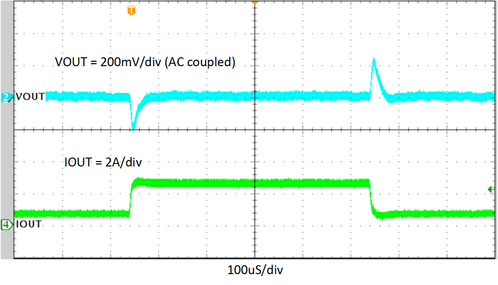
Figure 10-20 Load Transient Response, 1 to 3 A, Slew Rate = 0.8 A/μS
Figure 10-22 VOUT Hard Short Recovery
Figure 10-3 Load Regulation
Figure 10-5 Switching Frequency vs Load Current
Figure 10-7 Loop Frequency Response, IOUT = 3 A, BW = 49.4 kHz, PM = 57°, GM = –12 dB
Figure 10-9 Start-Up Relative to VIN, IOUT = 3 A
Figure 10-11 Start-Up Through EN, IOUT = 3 A
Figure 10-13 Steady State, IOUT = 0 A
Figure 10-15 Steady State, IOUT = 0.5 A
Figure 10-17 Steady State, IOUT = 2 A
 Figure 10-19 Load Transient Response, 0.5 to 2.5 A, Slew Rate = 0.8 A/μS
Figure 10-21 VOUT Hard Short Protection