SLVSD52A October 2015 – January 2016 TPS63020-Q1
PRODUCTION DATA.
- 1 Features
- 2 Applications
- 3 Description
- 4 Typical Application Schematic
- 5 Revision History
- 6 Device Comparison Table
- 7 Pin Configuration and Functions
- 8 Specifications
- 9 Detailed Description
- 10Application and Implementation
- 11Power Supply Recommendations
- 12Layout
- 13Device and Documentation Support
- 14Mechanical, Packaging, and Orderable Information
パッケージ・オプション
メカニカル・データ(パッケージ|ピン)
- DSJ|14
サーマルパッド・メカニカル・データ
- DSJ|14
発注情報
1 Features
- Qualified for Automotive Applications
- AEC-Q100 Qualified with the Following Results:
- Input Voltage Range: 1.8 V to 5.5 V
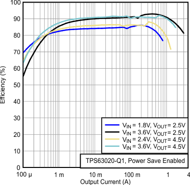
- Up to 96% Efficiency
- 3 A Output Current at 3.3 V in Step Down Mode (VIN > 3.6 V)
- More than 2 A Output Current at 3.3 V in Boost Mode (VIN > 2.5 V)
- Automatic Transition Between Step Down and Boost Mode
- Dynamic Input Current Limit
- Device Quiescent Current less than 50 μA
- Adjustable Output Voltage Range from 1.2 V to 5.5 V
- Power Save Mode for Improved Efficiency at Low Output Power
- Forced Fixed Frequency Operation at 2.4 MHz and Synchronization Possible
- Smart Power Good Output
- Load Disconnect During Shutdown
- Overtemperature Protection
- Overvoltage Protection
- Available in a 3-mm × 4-mm, VSON-14 Package
2 Applications
- Infotainment
- Telematics/eCall
3 Description
The TPS63020-Q1 device provides a power supply solution for products powered by either a two-cell or three-cell alkaline, NiCd or NiMH battery, or a one-cell Li-Ion or Li-Polymer battery. Output currents can go as high as 3 A while using a single-cell Li-Ion or Li-Polymer battery, and discharge it down to 2.5 V or lower. The buck-boost converter is based on a fixed frequency, pulse width modulation (PWM) controller using synchronous rectification to obtain maximum efficiency. At low load currents, the converter enters power save mode to maintain high efficiency over a wide load current range. The power save mode can be disabled, forcing the converter to operate at a fixed switching frequency. The maximum average current in the switches is limited to a typical value of 4 A. The output voltage is programmable using an external resistor divider. The converter can be disabled to minimize battery drain. During shutdown, the load is disconnected from the battery. The device is packaged in a 3 mm × 4 mm 14-pin VSON PowerPAD™ package (DSJ).
Device Information(1)
| PART NUMBER | PACKAGE | BODY SIZE (NOM) |
|---|---|---|
| TPS63020-Q1 | VSON (14) | 3.00 mm x 4.00 mm |
- For all available packages, see the orderable addendum at the end of the data sheet.

