JAJSCD1B June   2016  – March 2019 TPS63070

PRODUCTION DATA.  

  1. 特長
  2. アプリケーション
  3. 概要
    1.     Device Images
      1.      概略回路図
      2.      効率と出力電流との関係、、Vo = 5V
  4. 改訂履歴
  5. Device Comparison Table
  6. Pin Configuration and Functions
    1.     Pin Functions
  7. Specifications
    1. 7.1 Absolute Maximum Ratings
    2. 7.2 ESD Ratings
    3. 7.3 Recommended Operating Conditions
    4. 7.4 Thermal Information
    5. 7.5 Electrical Characteristics
    6. 7.6 Typical Characteristics
  8. Detailed Description
    1. 8.1 Overview
    2. 8.2 Functional Block Diagram TPS63070
    3. 8.3 Functional Block Diagram TPS630701
    4. 8.4 Feature Description
      1. 8.4.1  Control Loop Description
      2. 8.4.2  Precise Enable
      3. 8.4.3  Power Good
      4. 8.4.4  Soft Start
      5. 8.4.5  PS/SYNC
      6. 8.4.6  Short Circuit Protection
      7. 8.4.7  VSEL and FB2 pins
      8. 8.4.8  Overvoltage Protection
      9. 8.4.9  Undervoltage Lockout
      10. 8.4.10 Overtemperature Protection
    5. 8.5 Device Functional Modes
      1. 8.5.1 Power Save Mode
      2. 8.5.2 Current Limit
      3. 8.5.3 Output Discharge Function (TPS630702 only)
  9. Application and Implementation
    1. 9.1 Application Information
    2. 9.2 Typical Application for adjustable version
      1. 9.2.1 Design Requirements
      2. 9.2.2 Detailed Design Procedure
        1. 9.2.2.1 Programming The Output Voltage
        2. 9.2.2.2 Inductor Selection
        3. 9.2.2.3 Capacitor Selection
          1. 9.2.2.3.1 Input Capacitor
          2. 9.2.2.3.2 Output Capacitor
      3. 9.2.3 Application Curves
    3. 9.3 Typical Application for Fixed Voltage Version
      1. 9.3.1 Design Requirements
      2. 9.3.2 Detailed Design Procedure
      3. 9.3.3 Application Curves
  10. 10Power Supply Recommendations
    1. 10.1 Thermal Information
  11. 11Layout
    1. 11.1 Layout Guidelines
    2. 11.2 Layout Example
  12. 12デバイスおよびドキュメントのサポート
    1. 12.1 デバイス・サポート
      1. 12.1.1 デベロッパー・ネットワークの製品に関する免責事項
    2. 12.2 関連リンク
    3. 12.3 ドキュメントの更新通知を受け取る方法
    4. 12.4 コミュニティ・リソース
    5. 12.5 商標
    6. 12.6 静電気放電に関する注意事項
    7. 12.7 Glossary
  13. 13メカニカル、パッケージ、および注文情報

パッケージ・オプション

メカニカル・データ(パッケージ|ピン)
サーマルパッド・メカニカル・データ
発注情報

Pin Configuration and Functions

QFN PACKAGE
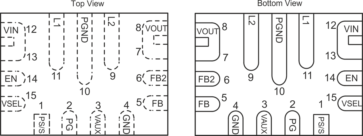
TPS63070 TPS63070_pinout_top_bottom.gif

Pin Functions

PIN I/O DESCRIPTION
NAME NO.
EN 14 I Enable input. Pull high to enable the device, pull low to disable the device.
FB 5 I Voltage feedback of adjustable versions, must be connected to VOUT on fixed output voltage versions
GND 4 Control / logic ground
L1 11 I Connection for Inductor
L2 9 I Connection for Inductor
PS/SYNC 1 I Pull to low for forced PWM, pull high for PWM/PFM (power save) mode. Apply a clock signal to synchronize to an external frequency.
PG 2 O Open drain power good output
PGND 10 Power ground
VIN 12, 13 I Supply voltage for power stage
VOUT 7,8 O Buck-boost converter output
VAUX 3 O Connection for Capacitor of internal voltage regulator. This pin must not be loaded externally.
VSEL 15 I Voltage scaling input. A high level on this pin enables a transistor which pulls pin FB2 to GND.
FB2 6 O Voltage scaling output. Connect a resistor from FB to FB2 to change the voltage divider ratio on the feedback pin. A logic high level on VSEL will change the output voltage to a higher value. Leave the pin open or connect to GND if not used.