SLVS504B March 2004 – September 2015 TPS65012
PRODUCTION DATA.
- 1 Features
- 2 Applications
- 3 Description
- 4 Revision History
- 5 Pin Configuration and Functions
- 6 Specifications
-
7 Detailed Description
- 7.1 Overview
- 7.2 Functional Block Diagram
- 7.3
Feature Description
- 7.3.1
Battery Charger
- 7.3.1.1 Autonomous Power Source Selection
- 7.3.1.2 Temperature Qualification
- 7.3.1.3 Battery Preconditioning
- 7.3.1.4 Battery Charge Current
- 7.3.1.5 Battery Voltage Regulation
- 7.3.1.6 Charge Termination and Recharge
- 7.3.1.7 Sleep Mode
- 7.3.1.8 PG Output
- 7.3.1.9 Thermal Considerations for Setting Charge Current
- 7.3.2 Step-Down Converters, VMAIN and VCORE
- 7.3.3 Low-Dropout Voltage Regulators
- 7.3.4 Undervoltage Lockout
- 7.3.5 Power-Up Sequencing
- 7.3.6 System Reset and Control Signals
- 7.3.7 Vibrator Driver
- 7.3.1
Battery Charger
- 7.4 Device Functional Modes
- 7.5 Programming
- 7.6
Register Maps
- 7.6.1 CHGSTATUS Register (Address: 01h—Reset: 00h)
- 7.6.2 REGSTATUS Register (Address: 02h—Reset: 00h)
- 7.6.3 MASK1 Register (Address: 03h—Reset: FFh)
- 7.6.4 MASK2 Register (Address: 04h—Reset: FFh)
- 7.6.5 ACKINT1 Register (Address: 05h—Reset: 00h)
- 7.6.6 ACKINT2 Register (Address: 06h—Reset: 00h)
- 7.6.7 CHGCONFIG Register Address: 07h—Reset: 1Bh
- 7.6.8 LED1_ON Register (Address: 08h—Reset: 00h)
- 7.6.9 LED1_PER Register (Address: 09h—Reset: 00h)
- 7.6.10 LED2_ON Register (Address: 0Ah—Reset: 00h)
- 7.6.11 LED2_PER (Register Address: 0Bh—Reset: 00h)
- 7.6.12 VDCDC1 Register (Address: 0Ch—Reset: 72h/73h)
- 7.6.13 VDCDC2 Register (Address: 0Dh—Reset: 68h/78h)
- 7.6.14 VREGS1Register (Address: 0Eh—Reset: 88h)
- 7.6.15 MASK3 Register (Address: 0Fh—Reset: 00h)
- 7.6.16 DEFGPIO Register Address: (10h—Reset: 00h)
- 8 Application and Implementation
- 9 Power Supply Recommendations
- 10Layout
- 11Device and Documentation Support
- 12Mechanical, Packaging, and Orderable Information
パッケージ・オプション
メカニカル・データ(パッケージ|ピン)
- RGZ|48
サーマルパッド・メカニカル・データ
- RGZ|48
発注情報
8 Application and Implementation
NOTE
Information in the following applications sections is not part of the TI component specification, and TI does not warrant its accuracy or completeness. TI’s customers are responsible for determining suitability of components for their purposes. Customers should validate and test their design implementation to confirm system functionality.
8.1 Application Information
The VCORE and VMAIN converter are always enabled in a typical application. The VCORE output voltage can be disabled or reduced from 1.5 V to a lower, preset voltage under processor control. When the processor enters the sleep mode, a high signal on the LOW_PWR pin initiates the change.
VCORE typically supplies the digital part of the audio codec. When the processor is in sleep or low-power mode, the audio codec is powered off, so the VCORE voltage can be programmed to lower voltages without a problem. A typical audio codec (e.g., TI AIC23) consumes about 20-mA to 30-mA current from the VCORE power supply.
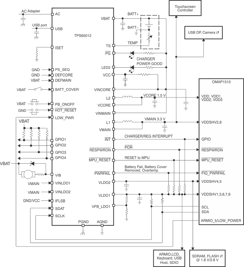
Supply LDO1 from VMAIN as shown in Figure 46. If this is not done, then subsequent to a UVLO, OVERTEMP, or BATT_COVER = 0 condition, the RESPWRON signal goes high before the VCORE rail has ramped and stabilized. Therefore, the processor core does not receive a power-on-reset signal.
8.2 Typical Applications
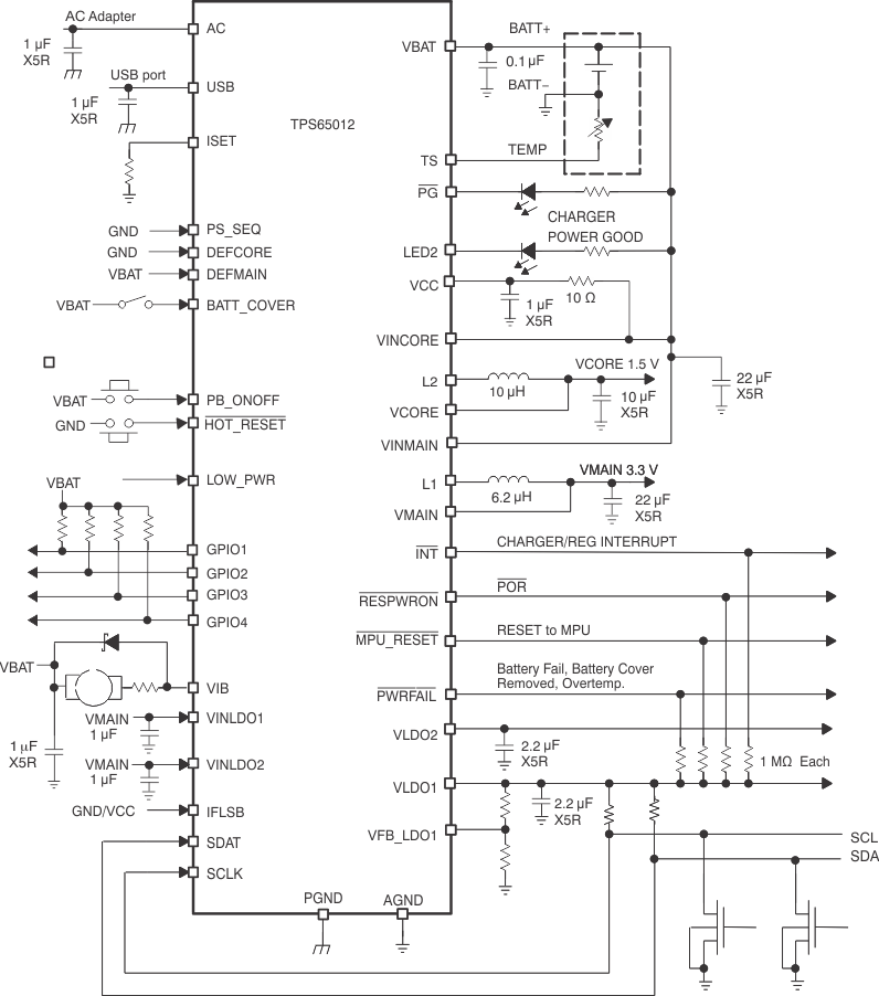
8.2.1 TPS65012 Typical Application
 Figure 43. Typical Application Circuit
8.2.1.1 Design Requirements
Each DC/DC converter requires an external inductor and filter capacitor, capable of sustain the intended current with an acceptable voltage ripple. LDOs must have external filter capacitors, and LDO1 requires an external feedback network for regulation. Every input supply rail requires a decoupling capacitor close to the pin, and to avoid unintended states, logic inputs without internal resistors must not be left floating.
8.2.1.2 Detailed Design Procedure
8.2.1.2.1 Inductor Selection for the Main and the Core Converter
The main and the core converters in the TPS65012 typically use a 6.2-µH and a 10-µH output inductor, respectively. Larger or smaller inductor values can be used to optimize the performance of the device for specific operation conditions. The selected inductor has to be rated for its DC resistance and saturation current. The DC resistance of the inductance influences directly the efficiency of the converter. Therefore, an inductor with lowest DC resistance is selected for highest efficiency.
Equation 3 calculates the maximum inductor current under static load conditions. The saturation current of the inductor should be rated higher than the maximum inductor current as calculated with Equation 3. This is needed because during heavy load transient, the inductor current rises above the value calculated under Equation 3.


where
- f = Switching frequency (1.25 MHz typical)
- L = Inductor value
- ΔIL= Peak-to-peak inductor ripple current
- ILmax = Maximum inductor current
The highest inductor current occurs at maximum VI.
Open core inductors have a soft saturation characteristic, and they can usually handle higher inductor currents versus a comparable shielded inductor.
A more conservative approach is to select the inductor current rating just for the maximum switch current of the TPS65012 (2 A for the main converter and 0.8 A for the core converter). Keep in mind that the core material from inductor to inductor differs and has an impact on the efficiency especially at high switching frequencies.
See Table 31 and the typical applications for possible inductors
Table 31. Tested Inductors
| DEVICE | INDUCTOR VALUE | DIMENSIONS | COMPONENT SUPPLIER |
|---|---|---|---|
| Core converter | 10 µH | 6,0 mm × 6,0 mm × 2,0 mm | Sumida CDRH5D18-100 |
| 10 µH | 5,0 mm × 5,0 mm × 3,0 mm | Sumida CDRH4D28-100 | |
| Main converter | 4.7 µH | 5,5 mm × 6,6 mm*1,0 mm | Coilcraft LPO1704-472M |
| 4.7 µH | 5,0 mm × 5,0 mm × 3,0 mm | Sumida CDRH4D28C-4.7 | |
| 4.7 µH | 5,2 mm × 5,2 mm × 2,5 mm | Coiltronics SD25-4R7 | |
| 5.3 µH | 5,7 mm × 5,7 mm × 3,0 mm | Sumida CDRH5D28-5R3 | |
| 6.2 µH | 5,7 mm × 5,7 mm × 3,0 mm | Sumida CDRH5D28-6R2 | |
| 6.0 µH | 7,0 mm × 7,0 mm × 3,0 mm | Sumida CDRH6D28-6R0 |
8.2.1.2.2 Output Capacitor Selection
The advanced fast response voltage mode control scheme of the inductive converters implemented in the TPS65012 allow the use of small ceramic capacitors with a typical value of 22 µF for the main converter and 10 µF for the core converter without having large output voltage under and overshoots during heavy load transients. Ceramic capacitors having low ESR values have the lowest output voltage ripple and are recommended. If required, tantalum capacitors with an ESR < 100 Ω resistance may be used as well.
See Table 32 for recommended components.
If ceramic output capacitors are used, the capacitor RMS ripple current rating must meet the application requirements. For completeness, the RMS ripple current is calculated as:

At nominal load current, the inductive converters operate in PWM mode and the overall output voltage ripple is the sum of the voltage spike caused by the output capacitor ESR plus the voltage ripple caused by charging and discharging the output capacitor:

Where the highest output voltage ripple occurs at the highest input voltage VI.
At light load currents, the converters operate in power-save mode, and the output voltage ripple is independent of the output capacitor value. The output voltage ripple is set by the internal comparator thresholds. The typical output voltage ripple is 1% of the nominal output voltage. If the output voltage for the core converter is programmed to its lowest voltage of 0.85 V, the output capacitor must be increased to 22 µF for low output voltage ripple. This is because the current in the inductor decreases slowly during the off-time and further increases the output voltage even when the PMOS is off. This effect increases with low output voltages.
8.2.1.2.3 Input Capacitor Selection
A pulsating input current is the nature of the buck converter. Therefore, a low ESR input capacitor is required for best input voltage filtering. It also minimizes the interference with other circuits caused by high input voltage spikes. The main converter needs a 22-µF ceramic input capacitor and the core converter a 10-µF ceramic capacitor. The input capacitor for the main and the core converter can be combined and one 22-µF capacitor can be used instead, because the two converters operate with a phase shift of 270 degrees. The input capacitor can be increased without any limit for better input voltage filtering. The VCC pin should be separated from the input for the main and the core converter. A filter resistor of up to 100 Ω and a 1-µF capacitor is used for decoupling the VCC pin from switching noise.
Table 32. Possible Capacitors
| CAPACITOR VALUE | CASE SIZE | COMPONENT SUPPLIER | COMMENTS |
|---|---|---|---|
| 22 µF | 1206 | TDK C3216X5R0J226M | Ceramic |
| 22 µF | 1206 | Taiyo Yuden JMK316BJ226ML | Ceramic |
| 22 µF | 1210 | Taiyo Yuden JMK325BJ226MM | Ceramic |
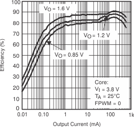
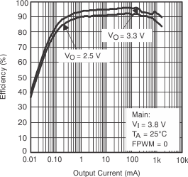
8.2.1.3 Application Curves
 Figure 44. Efficiency vs Output Current
 Figure 45. Efficiency vs Output Current
8.2.2 Low-Power Mode
 Figure 46. Typical Application Circuit in Low-Power Mode
8.2.2.1 Design Requirements
Use external logic or processor to control LOW_PWR state.