-
TPS65055 2.25-MHz Dual Step-Down Converter With 4 Low-Input Voltage LDOs
- 1 Features
- 2 Applications
- 3 Description
- 4 Revision History
- 5 Pin Configuration and Functions
- 6 Specifications
- 7 Parameter Measurement Information
- 8 Detailed Description
- 9 Application and Implementation
- 10Power Supply Recommendations
- 11Layout
- 12Device and Documentation Support
- 13Mechanical, Packaging, and Orderable Information
- IMPORTANT NOTICE
パッケージ・オプション
メカニカル・データ(パッケージ|ピン)
- RSM|32
サーマルパッド・メカニカル・データ
- RSM|32
発注情報
TPS65055 2.25-MHz Dual Step-Down Converter With 4 Low-Input Voltage LDOs
1 Features
- Up to 95% Efficiency
- Output Current for DCDC Converters 2 × 0.6 A
- Two Selectable Fixed Output Voltages 1 V and 1.2 V for DCDC2
- VIN Range for DCDC Converters From 2.5 V to 6 V
- 2.25-MHz Fixed-Frequency Operation
- Power Save Mode at Light Load Current
- 180° Out-of-Phase Operation
- Output Voltage Accuracy in PWM Mode ±1%
- Low Ripple PFM Mode
- Total Typical 32-μA Quiescent Current for Both DC-DC Converters
- 100% Duty Cycle for Lowest Dropout
- 2 General-Purpose 400 mA High PSRR LDOs
- 2 General-Purpose 200 mA High PSRR LDOs
- VIN Range for LDOs From 1.5 V to 6.5 V
- Digital Voltage Selection for the LDOs
- I2C Compatible Interface
- Available in a 4 mm × 4 mm 32-Pin QFN Package
2 Applications
- Cell Phones, Smart Phones
- WLAN
- PDAs, Pocket PCs
- OMAP™ and Low Power DSP Supplies
- XScale
- Portable Media Players
- Digital Cameras
3 Description
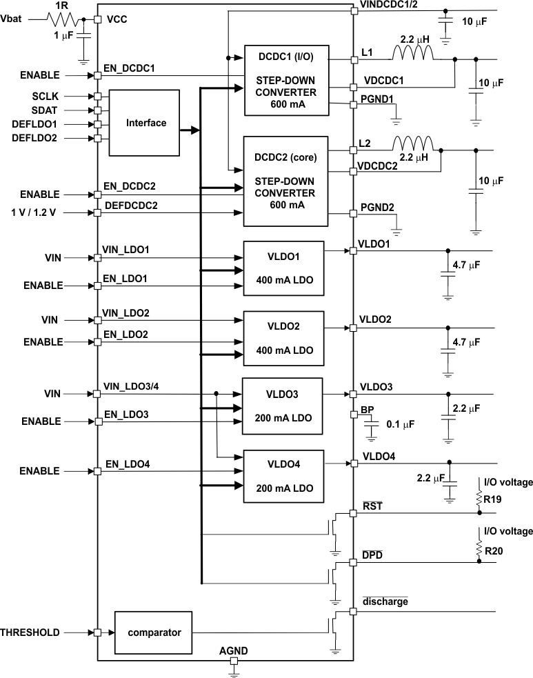
The TPS65055 device is an integrated Power Management IC for applications powered by one Li-Ion or Li-Polymer cell, which require multiple power rails.
The TPS65055 provides two highly efficient,
2.25 MHz step-down converters targeted at providing the core voltage and I/O voltage in a processor-based system. Both step-down converters enter a low power mode at light load for maximum efficiency across the widest possible range of load currents.
For low noise applications the device can be forced into fixed frequency PWM mode using the I2C compatible interface. In shutdown mode, current consumption is reduced to less than 1 μA.
The device allows the use of small inductors and capacitors to achieve a small solution size.
The TPS65055 provides an output current of up to 0.6 A on each DC-DC converter.
The TPS65055 also integrates two 400-mA LDO and two 200-mA LDO voltage regulators, which can be turned on/off using separate enable pins on each LDO. Each LDO operates with an input voltage range from 1.5 V to 6.5 V allowing them to be supplied from one of the step-down converters or directly from the main battery. Two digital input pins are used to set the output voltage of the LDOs from a set of 9 different combinations for LDO1 to LDO4. Additionally, the converters can be controlled by an I2C compatible interface.
The TPS65055 is available in a small 32-pin leadless package (4 mm × 4 mm QFN) with a 0.4-mm pitch.
Device Information(1)
| PART NUMBER | PACKAGE | BODY SIZE (NOM) |
|---|---|---|
| TPS65055 | VQFN (32) | 4.00 mm × 4.00 mm |
- For all available packages, see the orderable addendum at the end of the data sheet.
Block Diagram

4 Revision History
Changes from * Revision (September 2008) to A Revision
- Added ESD Ratings table, Feature Description section, Device Functional Modes, Application and Implementation section, Power Supply Recommendations section, Layout section, Device and Documentation Support section, and Mechanical, Packaging, and Orderable Information sectionGo
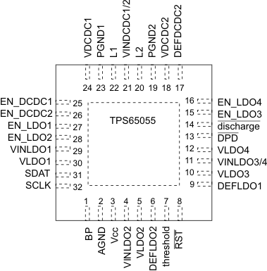
5 Pin Configuration and Functions

Pin Functions
| PIN | I/O | DESCRIPTION | |
|---|---|---|---|
| NAME | NO. | ||
| AGND | 2 | I | Analog GND, connect to PGND and PowerPAD |
| BP | 1 | I | Input for bypass capacitor for internal reference |
| DEF_DCDC2 | 17 | I | Select pin of converter 2 output voltage. High = 1 V, low = 1.2 V |
| DEFLDO1 | 9 | I | Digital input, used to set the default output voltage of LDO1 to LDO4; LSB |
| DEFLDO2 | 6 | I | Digital input, used to set the default output voltage of LDO1 to LDO4; MSB |
| discharge | 14 | O | Open-drain output driven by the signal at the threshold input |
| DPD | 13 | O | Open-drain active low output; low after UVLO event |
| EN_DCDC1 | 25 | I | Enable input for converter1, active high |
| EN_DCDC2 | 26 | I | Enable input for converter2, active high |
| EN_LDO1 | 27 | I | Enable input for LDO1. Logic high enables the LDO, logic low disables the LDO. |
| EN_LDO2 | 28 | I | Enable input for LDO2. Logic high enables the LDO, logic low disables the LDO. |
| EN_LDO3 | 15 | I | Enable input for LDO3. Logic high enables the LDO, logic low disables the LDO. |
| EN_LDO4 | 16 | I | Enable input for LDO4. Logic high enables the LDO, logic low disables the LDO. |
| L1 | 22 | O | Switch pin of converter1. Connected to inductor |
| L2 | 20 | O | Switch pin of converter 2. Connected to inductor. |
| PGND1 | 23 | I | GND for converter 1 |
| PGND2 | 19 | I | GND for converter 2 |
| RST | 8 | O | Open-drain active low output; low after UVLO event |
| SCLK | 32 | I | Clock input for the I2C compatible interface. |
| SDAT | 31 | I/O | Data line for the I2C compatible interface. |
| threshold | 7 | I | Input to comparator driving the discharge output. If the input voltage at threshold is < 0.8 V, the discharge output is actively pulled low. |
| Vcc | 3 | I | Power supply for digital and analog circuitry of DCDC1, DCDC2 and LDOs. This pin must be connected to the same voltage supply as VINDCDC1/2. |
| VDCDC1 | 24 | I | Feedback voltage sense input, connect directly to Vout1 |
| VDCDC2 | 18 | I | Feedback voltage sense input, connect directly to Vout2 |
| VINDCDC1/2 | 21 | Input voltage for VDCDC1 and VDCDC2 step-down converter. This must be connected to the same voltage supply as VCC. | |
| VINLDO1 | 29 | I | Input voltage for LDO1 |
| VINLDO2 | 4 | I | Input voltage for LDO2 |
| VINLDO3/4 | 11 | I | Input voltage for LDO3 and LDO4 |
| VLDO1 | 30 | O | Output voltage of LDO1 |
| VLDO2 | 5 | O | Output voltage of LDO2 |
| VLDO3 | 10 | O | Output voltage of LDO3 |
| VLDO4 | 12 | O | Output voltage of LDO4 |
| PowerPAD™ | – | Connect to GND | |