SLVSBO6B January 2013 – July 2015 TPS65090
PRODUCTION DATA.
- 1 Features
- 2 Applications
- 3 Description
- 4 Revision History
- 5 Pin Configuration and Functions
-
6 Specifications
- 6.1 Absolute Maximum Ratings
- 6.2 ESD Ratings
- 6.3 Recommended Operating Conditions
- 6.4 Thermal Information
- 6.5 Electrical Characteristics - Power Path Control
- 6.6 Electrical Characteristics - Charger
- 6.7 Electrical Characteristics - DC-DC Converters
- 6.8 Electrical Characteristics - Linear Regulators
- 6.9 Electrical Characteristics - Load Switches
- 6.10 Electrical Characteristics - Control
- 6.11 Timing Requirements - I2C Interface
- 6.12 Typical Characteristics
- 7 Detailed Description
-
8 Application and Implementation
- 8.1 Application Information
- 8.2
Typical Applications
- 8.2.1
Front-End PMU Application
- 8.2.1.1 Design Requirements
- 8.2.1.2
Detailed Design Procedure
- 8.2.1.2.1 Programming the Converter or Charger Output Voltage
- 8.2.1.2.2 Programming Input DPM Current and Charge Current
- 8.2.1.2.3 Output Filter Design (Inductor and Output Capacitor)
- 8.2.1.2.4 Inductor Selection
- 8.2.1.2.5 Capacitor Selection
- 8.2.1.2.6 Charger Battery Temperature Sensing
- 8.2.1.2.7 Reverse Voltage Protection
- 8.2.1.2.8 AC Switches
- 8.2.1.2.9 Battery Switches
- 8.2.1.3 Application Curves
- 8.2.2 DC-DC Converters
- 8.2.3 Charger
- 8.2.1
Front-End PMU Application
- 9 Power Supply Recommendations
- 10Layout
- 11Device and Documentation Support
- 12Mechanical, Packaging, and Orderable Information
パッケージ・オプション
メカニカル・データ(パッケージ|ピン)
- RVN|100
サーマルパッド・メカニカル・データ
- RVN|100
発注情報
8 Application and Implementation
NOTE
Information in the following applications sections is not part of the TI component specification, and TI does not warrant its accuracy or completeness. TI’s customers are responsible for determining suitability of components for their purposes. Customers should validate and test their design implementation to confirm system functionality.
8.1 Application Information
The TPS65090A front-end PMU integrated circuit is intended for systems powered by a 2- or 3-cell Li-Ion or Li-Polymer battery with a typical voltage from 6 V to 17 V. Additionally, any other voltage source with a typical output voltage from 6 V to 7 V can power systems where the TPS65090A is used.
8.2 Typical Applications
8.2.1 Front-End PMU Application
 Figure 46. Front-End PMU Application Diagram
8.2.1.1 Design Requirements
For this design example, use the parameters listed in Table 28 as the input parameters.
Table 28. Design Parameters
| PARAMETER | EXAMPLE VALUE |
|---|---|
| Input voltage range (VAC) | 6 V to 17 V |
| VLDO1 | 5 V (on by default) |
| VLDO2 | 3.3 V (on by default) |
| DCDC1 | 5 V (off by default) |
| DCDC2 | 3.3 V (off by default) |
| DCDC3 | 3.3 V (off by default) |
8.2.1.2 Detailed Design Procedure
8.2.1.2.1 Programming the Converter or Charger Output Voltage
Within the TPS65090A device, there are fixed and adjustable outputs. In the case where the voltage is adjustable, an external resistor divider is used to set the output voltage. The resistor divider must be connected between the output, the feedback pin and GND. When the output voltage is regulated properly, the voltage at the feedback pin will be in the range as defined in Electrical Characteristics, that is, 800 mV for DCDC3 and 2.1 V for the charger. The feedback pin typically has 0.1 μA of leakage; to meet this current requirement and maintain the feedback voltage, TI recommends setting the feedback divider current by at least a factor of ten to one-hundred times that of the pin leakage. Using the feedback voltage of 2.1 V and 10 μA (100 × 0.1 μA), the resistor between the feedback pin and GND can be calculated to be less than 210 kΩ. This value for the resistor will provide sufficient current through the resistor divider at the typical feedback voltage. Selecting resistor values is a trade off between noise immunity and light load efficiency. The lower the resistor value, the higher the noise immunity; however, the more current through the resistor, the less efficient the converter is at light loads. Consider R1 is connected from the output of the inductor to the feedback pin and R2 from the feedback pin to ground. From the recommendations for R2, less than 210 kΩ, the value of the resistor connected between the output and feedback, R1, depending on the desired output voltage VOUT, can be calculated using Equation 1.

Table 29 contains recommended values for the feedback divider for the most common output voltages.
Table 29. Feedback Resistor Values for Common Converter Output Voltages
| OUTPUT VOLTAGE | 1.2 V | 1.35 V | 1.8 V | 3.3 V |
|---|---|---|---|---|
| R1 [kΩ] | 260 | 330 | 510 | 750 |
| R2 [kΩ] | 510 | 470 | 400 | 240 |
Table 30. Feedback Resistor Values for Common Charger Output Voltages
| OUTPUT VOLTAGE | 8.4 V | 12.6 V |
|---|---|---|
| R1 [kΩ] | 330 | 1100 |
| R2 [kΩ] | 110 | 220 |
8.2.1.2.2 Programming Input DPM Current and Charge Current
Maximum input DPM current and charge current are defined by the values of the sense resistors used. The sense resistor value RS can be calculated using Equation 2.

VS is the differential voltage at the sense input pins. For input current DPM, it is the differential voltage between ACP and ACN, and for charge current regulation, between SRP and SRN. For the differential voltage, TI recommends a maximum value of 40 mV here. More details can be found in Electrical Characteristics - Power Path Control.
IS is the maximum current which must be controlled. For input current DPM, it is the maximum input current where charging is still allowed, and for charge current regulation, it is the maximum charge current.
8.2.1.2.3 Output Filter Design (Inductor and Output Capacitor)
The external components must fulfill the needs of the application, but also the stability criteria of the devices control loop. The is optimized to work within a range of L and C combinations. The LC output filter inductance and capacitance must be considered together, creating a double pole, responsible for the corner frequency of the converter.
8.2.1.2.4 Inductor Selection
At the L pins of the DC-DC converters and the charger, connecting an inductor is required.
At the DC-DC converters, TI recommends using a 2.2-μH inductor with an appropriate current rating for the application. The derated inductance at high currents should not drop lower than 1 μH.
At the charger, TI recommends using a 2.2-μH inductor for fast-charge currents of 3 A and above. For lower fast charge currents, 3.3 μH can be used. The current rating of the inductor must be suitable for the maximum fast-charge current required in the application.
The inductor value affects its peak-to-peak ripple current, the PWM-to-PSM transition point, the output voltage ripple, and the efficiency. The selected inductor must be rated for its DC resistance and saturation current. The inductor ripple current decreases with higher inductance and increases with higher VIN or VOUT.
To properly configure the converter, an inductor must be connected between pin L the output capacitors. To estimate the inductance value, Equation 3 can be used.

In Equation 3, the minimum inductance value, L, is calculated. VIN is the minimum input voltage. As an example, a suitable inductor for generating 1.35 V from a two-cell Li-Ion battery is 2.2 μH.
With the chosen inductance value, the peak current for the inductor in steady state operation can be calculated. Equation 4 shows how to calculate the peak current IMAX in step-down mode operation.

In the equation, f is the minimum switching frequency, which typically is in the range of 1 MHz. VIN is the minimum input voltage. The critical current value for selecting the right inductor is the value of IMAX. Consideration must be given to the load transients and error conditions that can cause higher inductor currents. This must be taken into consideration when selecting an appropriate inductor.
In DC-DC converter applications, the efficiency is essentially affected by the inductor AC resistance (that is, quality factor) and by the inductor DCR value. To achieve high-efficiency operation, care must be taken in selecting inductors featuring a quality factor greater than 25 at the switching frequency. Increasing the inductor value produces lower RMS currents, but degrades transient response. For a given physical inductor size, increased inductance usually results in an inductor with lower saturation current.
The following inductor types from different suppliers have been used with TPS65090 converters:
Table 31. List of Inductors
| VENDOR | INDUCTOR SERIES |
|---|---|
| Coilcraft | XAL4020-222, XAL5030-222 |
| Cyntec | PILE061E-2R2MS-11 |
| Toko | FDV0530-2R2M |
| Wurth Elektronik | WE 74437324022 |
8.2.1.2.5 Capacitor Selection
8.2.1.2.5.1 Input Capacitor
Because of the nature of the switching converter and charger with a pulsating input current, a low ESR input capacitor is required for best input voltage filtering and minimizing the interference with other circuits caused by high input voltage spikes. For most applications, TI recommends a ceramic capacitor of at least 10-µF. The voltage rating and DC bias characteristic of ceramic capacitors must be considered. The input capacitor can be increased without any limit for better input voltage filtering. TI recommends a ceramic capacitor placed as close as possible to the respective VSYS and PGND pins of the IC.
8.2.1.2.5.2 DC-DC Converter and Charger Bootstrap Capacitors
To make sure that the internal high side gate drivers are supplied with a stable low noise supply voltage, a capacitor must be connected between the CBx pins and the respective Lx pins.
TI recommends using a ceramic capacitor with a value of 4700 pF. The value of this capacitor should not be lower than 2200 pF or higher than 0.01 μF. For testing, a 4700-pF, size 0402, 6.3-V capacitor was used.
8.2.1.2.5.3 DC-DC Converter and Charger Output Capacitors
TI recommends ceramic capacitors with low ESR values that provide the lowest output voltage ripple. The output capacitor requires either an X7R or X5R dielectric. Y5V and Z5U dielectric capacitors, aside from their wide variation in capacitance overtemperature, become resistive at high frequencies.
At light load currents, the converter operates in power save mode and the output voltage ripple is dependent on the output capacitor value and the PFM peak inductor current. Higher output capacitor values minimize the voltage ripple in PFM Mode and tighten DC output accuracy in PFM Mode. To achieve specified regulation performance and low output voltage ripple, the DC-bias characteristic of ceramic capacitors must be considered. The effective capacitance of ceramic capacitors drops with increasing DC - bias voltage.
For the output capacitors of the DC-DC converters and the charger, TI recommends the use of small ceramic capacitors placed as close as possible to the output pins and the respective PGND pins of the IC. If, for any reason, the application requires the use of large capacitors which cannot be placed close to the IC, use a smaller ceramic capacitor in parallel to the large capacitor. The small capacitor should be placed as close as possible to the output pins and the respective PGND pins of the IC.
At the DC-DC converters, TI recommends the capacitance close to the IC to be close to 22 μF. It should not be lower than 10 μF or higher than 47 μF.
At the charger, TI recommends a 22-μF capacitance.
To get an estimate of the recommended minimum output capacitance, Equation 5 can be used.

A capacitor with a value in the range of or higher than the calculated minimum should be used. This is required to maintain control loop stability.
8.2.1.2.5.4 LDO Output Capacitors
To achieve stable and accurate output voltage regulation of the LDO's, a small ceramic capacitor is required at their outputs. TI recommends using at least 2.2 μF.
8.2.1.2.5.5 Load Switches Output Capacitors
The maximum expected output capacitance at the load switches is 47 μF. Any lower value can be used.
8.2.1.2.6 Charger Battery Temperature Sensing
To measure the battery cell temperature, resistors with temperature dependent resistance (NTC) must be placed close to the cells which must be measured. The device supports using two independent measuring points with its TS1 and TS2 input pins. The temperature sense resistor and the linearizing resistor network must be the same. If only one temperature sense resistor is used, the sense resistor network must be connected to TS1 and TS2.
As a default, the internal circuit is optimized to work with a 10-kΩ NTC resistor with a temperature characteristic described with a B value in the range of 3450 with one resistor in parallel and one resistor in series for linearization and to define the resistor-divider connected to VREFT, TSx and AGND. A possible default example would be NTCS0805E3103FLT from Vishay in parallel with a 6.8-kΩ resistor and a 2.2-kΩ resistor in series.
8.2.1.2.7 Reverse Voltage Protection
To protect the design against reverse voltage at the AC adapter input, additional external components are required. The pins VAC, VACS and the input path switches are exposed to the negative voltage and need some protection.
To protect the VAC pin, TI recommends using a small signal diode between the adapter input and the VAC pin.
Protecting VACS can be done either by connecting this pin to the protected VAC with the tradeoff of losing accuracy or connecting VACS to the adapter input with a 10-kΩ resistor.
To make sure that the AC switches are not turned on with the reverse voltage at the AC adapter input, a small signal N-channel FET can be used to short the voltage at ACG to ACS. The source of this FET must be connected to ACS, the drain to ACG. The gate must be connected to the AC adapter input GND either direct, or if the maximum gate voltage rating does not match the maximum input voltage, with a resistor-divider between AC adapter input GND and ACS. An example for the small signal FET would be BSS138W-7-F. To protect the ACS and the ACG pin resistors with values in the range of 4.7 kΩ or higher between the pins and the gate and source pins of the AC FET's must be used.
An example for this additional reverse protection circuit can be found in the TPS65090EVM User's Guide, SLVU778.
8.2.1.2.8 AC Switches
The AC adapter protection switches are recommended as CSD17304Q3: MOSFET, NChan, 30 V, 56 A, 9.8 mΩ.
8.2.1.2.9 Battery Switches
The battery switches are recommended as CSD25401Q3: MOSFET, PChan, –20 V, 60 A, 8.7 mΩ.
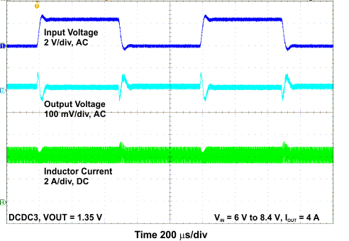
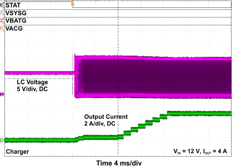
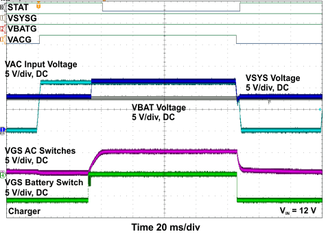
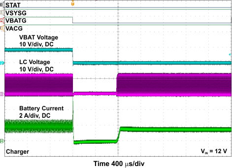
8.2.1.3 Application Curves


8.2.2 DC-DC Converters
 Figure 69. DC-DC Converters Circuit Drawing
Table 32. List of Components - DCDC1
| REFERENCE | DESCRIPTION | MANUFACTURER |
|---|---|---|
| L | 2.2 μH, 5 mm × 5 mm × 3 mm | XAL5030-222, Coilcraft |
| CIN | 10 μF, 25 V, 0603, X7R ceramic in parallel to | GRM188R61E106ME73, Murata |
| 1 μF, 25 V, 0402, X7R ceramic | GRM155R61E105MA12, Murata | |
| COUT | 4 × 10 μF, 25 V, 0603, X7R ceramic in parallel to | GRM188R61E106ME73, Murata |
| 2.2 μF 10 V, 0603, X7R ceramic | GRM155R61A225KE95, Murata | |
| CB1 | 4700 pF, X7R ceramic | |
| RFB1 | Not used, FB1 is directly connected to VDCDC1 | |
| RFB2 | Not used | |
Table 33. List of Components - DCDC2
| REFERENCE | DESCRIPTION | MANUFACTURER |
|---|---|---|
| L | 2.2 μH, 5 mm × 5 mm × 3 mm | XAL5030-222, Coilcraft |
| CIN | 10 μF, 25 V, 0603, X7R ceramic in parallel to | GRM188R61E106ME73, Murata |
| 1 μF, 25 V, 0402, X7R ceramic | GRM155R61E105MA12, Murata | |
| COUT | 4 × 10 μF, 25 V, 0603, X7R ceramic in parallel to | GRM188R61E106ME73, Murata |
| 2.2 μF 10 V, 0603, X7R ceramic | GRM155R61A225KE95, Murata | |
| CB2 | 4700 pF, X7R ceramic | |
| RFB1 | Not used, FB2 is directly connected to VDCDC2 | |
| RFB2 | Not used | |
Table 34. List of Components - DCDC3
| REFERENCE | DESCRIPTION | MANUFACTURER | COMMENTS |
|---|---|---|---|
| L | 2.2 μH, 5 mm × 5 mm × 3 mm | XAL5030-222, Coilcraft | |
| CIN | 10 μF, 25 V, 0603, X7R ceramic in parallel to | GRM188R61E106ME73, Murata | |
| 1 μF, 25 V, 0402, X7R ceramic | GRM155R61E105MA12, Murata | ||
| COUT | 4 × 10 μF, 25 V, 0603, X7R ceramic in parallel to | GRM188R61E106ME73, Murata | |
| 2.2 μF 10 V, 0603, X7R ceramic | GRM155R61A225KE95, Murata | ||
| CB1 | 4700 pF, X7R ceramic | Any | |
| RFB1 | 162 kΩ, 1%, 0402 | Any | VDCDC3 = 1 V |
| 330 kΩ, 1%, 0402 | Any | VDCDC3 = 1.35 V | |
| 453 kΩ, 1%, 0402 | Any | VDCDC3 = 1.8 V | |
| 590 kΩ, 1%, 0402 | Any | VDCDC3 = 3.3 V | |
| 649 kΩ, 1%, 0402 | Any | VDCDC3 = 4 V | |
| 787 kΩ, 1%, 0402 | Any | VDCDC3 = 5 V | |
| RFB2 | 649 kΩ, 1%, 0402 | Any | VDCDC3 = 1 V |
| 470 kΩ, 1%, 0402 | Any | VDCDC3 = 1.35 V | |
| 365 kΩ, 1%, 0402 | Any | VDCDC3 = 1.8 V | |
| 187 kΩ, 1%, 0402 | Any | VDCDC3 = 3.3 V | |
| 162 kΩ, 1%, 0402 | Any | VDCDC3 = 4 V | |
| 150 kΩ, 1%, 0402 | Any | VDCDC3 = 5 V |
8.2.3 Charger
 Figure 70. Charger Circuit Drawing
Table 35. List of Components - Charger
| REFERENCE | DESCRIPTION | MANUFACTURER | COMMENTS |
|---|---|---|---|
| L | 2.2 μH, 5 mm × 5 mm × 3 mm | XAL5030-222, Coilcraft | |
| CIN | 2 × 10 μF, 25 V, 0603, X7R ceramic in parallel to | GRM188R61E106ME73, Murata | |
| 1 μF, 25 V, 0402, X7R ceramic | GRM155R61E105MA12, Murata | ||
| COUT | 2 × 10 μF, 25 V, 0603, X7R ceramic in parallel to | GRM188R61E106ME73, Murata | |
| 1 μF, 25 V, 0402, X7R ceramic | GRM155R61E105MA12, Murata | ||
| CBC | 4700 pF, X7R ceramic | Any | |
| RS | 10 mΩ, 0.1%, 1206 | Any | Maximum charge current 4 A |
| RFB1 | 330 kΩ, 1%, 0402 | Any | Charge termination voltage VBAT = 8.4 V |
| 1100 kΩ, 1%, 0402 | Any | Charge termination voltage VBAT = 12.6 V | |
| RFB2 | 110 kΩ, 1%, 0402 | Any | Charge termination voltage VBAT = 8.4 V |
| 220 kΩ, 1%, 0402 | Any | Charge termination voltage VBAT = 12.6 V |
