SLVS496D SEPTEMBER 2003 – August 2016 TPS65100 , TPS65101 , TPS65105
PRODUCTION DATA.
- 1 Features
- 2 Applications
- 3 Description
- 4 Revision History
- 5 Device Options
- 6 Pin Configuration and Functions
- 7 Specifications
- 8 Detailed Description
- 9 Application and Implementation
- 10Power Supply Recommendations
- 11Layout
- 12Device and Documentation Support
- 13Mechanical, Packaging, and Orderable Information
パッケージ・オプション
デバイスごとのパッケージ図は、PDF版データシートをご参照ください。
メカニカル・データ(パッケージ|ピン)
- RGE|24
- PWP|24
サーマルパッド・メカニカル・データ
発注情報
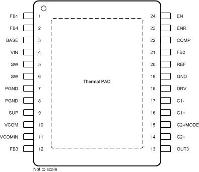
6 Pin Configuration and Functions
PWP Package
24-Pin HTSSOP
(Top View)

RGE Package
24-Pin VQFN
(Top View)

Pin Functions
| PIN | I/O | DESCRIPTION | ||
|---|---|---|---|---|
| NAME | HTSSOP | VQFN | ||
| BASE | 3 | 6 | O | Base drive output for the external transistor. If Linear Regulator is not needed pull this pin against VIN. |
| C1+ | 16 | 19 | — | Positive terminal of the charge pump flying capacitor |
| C1- | 17 | 20 | — | Negative terminal of the charge pump flying capacitor |
| C2+ | 14 | 17 | — | Positive terminal for the charge pump flying capacitor. If the device runs in voltage doubler mode, this pin should be left open. |
| C2-/MODE | 15 | 18 | — | Negative terminal of the charge pump flying capacitor and charge pump MODE pin. If the flying capacitor is connected to this pin, the converter operates in a voltage tripler mode. If the charge pump needs to operate in a voltage doubler mode, the flying capacitor is removed and the C2-/MODE pin should be connected to GND. |
| COMP | 22 | 1 | — | Compensation pin for the main boost converter. A small capacitor is connected to this pin. |
| DRV | 18 | 21 | O | External charge pump driver |
| EN | 24 | 3 | I | Enable pin of the device. This pin should be terminated and not be left floating. A logic high enables the device and a logic low shuts down the device. |
| ENR | 23 | 2 | I | Enable pin of the linear regulator controller. This pin should be terminated and not be left floating. Logic high enables the regulator and a logic low puts the regulator in shutdown. |
| FB1 | 1 | 4 | I | Feedback pin of the boost converter |
| FB2 | 21 | 24 | I | Feedback pin of negative charge pump |
| FB3 | 12 | 15 | I | Feedback pin of positive charge pump |
| FB4 | 2 | 5 | I | Feedback pin of the linear regulator controller. The linear regulator controller is set to a fixed output voltage of 3.3 V or 3 V depending on the version. |
| GND | 19 | 22 | — | Ground |
| OUT3 | 13 | 16 | O | Positive charge pump output |
| PGND | 7, 8 | 10, 11 | — | Power ground |
| REF | 20 | 23 | O | Internal reference output typically 1.23 V |
| SUP | 9 | 12 | I | Supply pin of the positive, negative charge pump, boost converter gate drive circuit, and VCOM buffer. This pin should be connected to the output of the main boost converter and cannot be connected to any other voltage source. For performance reasons, it is not recommended for a bypass capacitor to be connected directly to this pin. |
| SW | 5, 6 | 8, 9 | — | Switch pin of the boost converter |
| VCOM | 10 | 13 | O | VCOM buffer output |
| VCOMIN | 11 | 14 | I | Positive input terminal of the VCOM buffer. When the VCOM buffer is not used, this terminal can be connected to GND to reduce the overall quiescent current of the IC. |
| VIN | 4 | 7 | I | Input voltage pin of the device |
| PowerPAD™/ Thermal Die |
— | — | — | The PowerPAD or exposed thermal die needs to be connected to the power ground pins (PGND) |