SLVSC01A June 2013 – April 2015 TPS65133
PRODUCTION DATA.
- 1 Features
- 2 Applications
- 3 Description
- 4 Typical Application
- 5 Revision History
- 6 Pin Configuration and Functions
- 7 Specifications
- 8 Detailed Description
- 9 Application and Implementation
- 10Power Supply Recommendations
- 11Layout
- 12Device and Documentation Support
- 13Mechanical, Packaging, and Orderable Information
パッケージ・オプション
メカニカル・データ(パッケージ|ピン)
- DPD|12
サーマルパッド・メカニカル・データ
- DPD|12
発注情報
8 Detailed Description
8.1 Overview
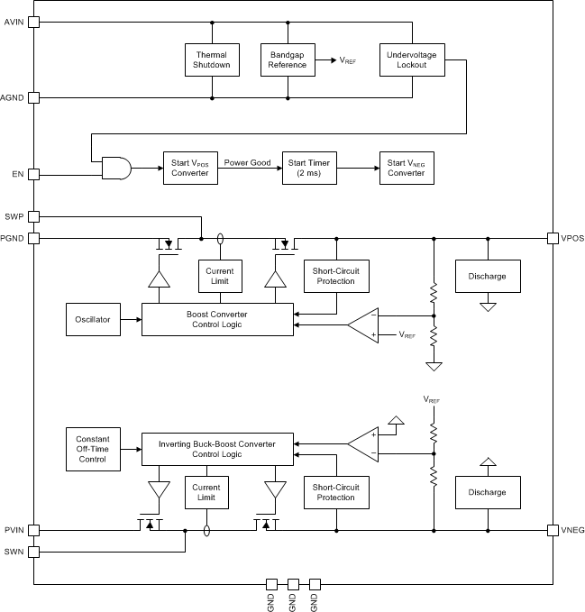
The TPS65133 device comprises a boost converter and an inverting buck-boost converter. The boost converter generates a positive output voltage of 5.0 V and the inverting buck-boost converter generates a negative output voltage of –5.0 V. Both converters have an output voltage accuracy of ±1%.
8.2 Functional Block Diagram

8.3 Feature Description
8.3.1 Boost Converter (VPOS)
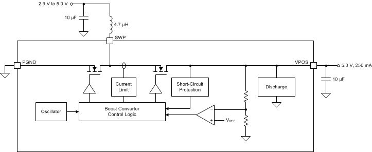
The boost converter uses a current-mode topology with synchronous rectification (see Figure 6). The synchronous rectifier improves efficiency and provides input-output isolation when the converter is disabled. When the input supply voltage is close 5.0 V, preventing normal boost operation, the synchronous rectifier is disabled, allowing the output voltage regulation to be maintained (see Operation with VI ≈ VPOS (Diode Mode)).
 Figure 6. VPOS Boost Converter Internal Block Diagram
8.3.1.1 Switching Frequency (VPOS)
The boost converter switching frequency may vary slightly as the operating conditions change, but is typically around 1.7 MHz for most operating conditions.
8.3.1.2 Output Voltage (VPOS)
The boost converter's output voltage is factory-programmed to 5.0 V ±1.0% and cannot be changed by the user.
8.3.1.3 Startup (VPOS)
The boost converter starts up as soon as EN=HIGH and the input supply voltage is above the UVLO threshold. The converter features an integrated soft-start function to control the ramp of its output voltage.
8.3.1.4 Shutdown (VPOS)
The boost converter shuts down when EN=LOW or the input supply voltage falls below the UVLO threshold.
8.3.1.5 Active Discharge (VPOS)
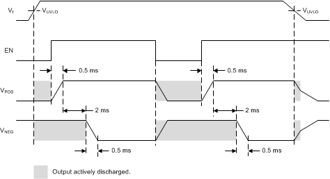
The boost converter output is actively discharged to ground when the converter is disabled (see Figure 8). During startup, active discharge begins as soon as the input supply voltage is above the UVLO threshold. During shutdown, active discharge persists until the input supply voltage is too low to support its operation (VI ≈ 1.5 V).
8.3.1.6 Short-Circuit Protection (VPOS)
The boost converter is protected against short-circuits on its output. If a short-circuit condition is detected during start-up, the converter limits its output current until the short-circuit condition is removed. Note that if a boost converter short-circuit condition is detected during start-up, the inverting buck-boost converter will not start until the condition is removed (because the sequencing logic requires VPOS to be in regulation before the inverting buck-boost converter is started).
During normal operation the boost converter detects a short-circuit on its output if VPOS < 4.1 V for longer than 3 ms. When a short-circuit condition is detected both VPOS and VNEG are disabled and the device shuts down. Normal operation is resumed by pulling EN low and then high again, or by cycling the input supply voltage.
8.3.2 Inverting Buck-Boost Converter (VNEG)
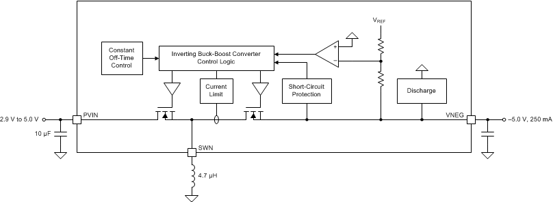
The inverting buck-boost converter uses a current-mode topology with synchronous rectification (see Figure 7).
 Figure 7. VNEG Buck-Boost Converter Internal Block Diagram
8.3.2.1 Switching Frequency (VNEG)
The inverting buck-boost converter's switching frequency varies slightly with operating conditions, but is approximately 1.7 MHz for most operating conditions.
8.3.2.2 Output Voltage (VNEG)
The inverting buck-boost converter's output voltage is factory-programmed to –5.0 V ±1.0% and cannot be changed by the user.
8.3.2.3 Startup (VNEG)
The inverting buck-boost converter starts up approximately 2 ms after the boost converter output has reached 5.0 V. The converter's switch current is limited during startup and the output voltage ramps in a controlled manner.
8.3.2.4 Shutdown
The inverting buck-boost converter shuts down when EN=LOW or the input supply voltage falls below the UVLO threshold.
8.3.2.5 Active Discharge (VNEG)
The inverting buck-boost converter output is actively discharged to ground when the converter is disabled (see Figure 8). During startup, active discharge begins as soon as the input supply voltage is above the UVLO threshold. During shutdown, active discharge persists until the input supply voltage is too low to support its operation (VI ≈ 1.5 V).
8.3.2.6 Short-Circuit Protection (VNEG)
The inverting buck-boost converter is protected against short-circuits on its output. If a short-circuit condition is detected during startup, the device converter limits its output current until the short-circuit condition is removed.
During normal operation the inverting buck-boost converter detects a short-circuit on its output if VNEG > –4.5 V for longer than 3 ms. When a short-circuit condition is detected both VPOS and VNEG are disabled and the device shuts down. Normal operation is resumed by pulling EN low and then high again, or by cycling the input supply voltage.
8.3.3 Startup and Shutdown Sequencing
Figure 8 illustrates the startup and shutdown sequencing of the TPS65133 device.
 Figure 8. Startup and Shutdown Sequencing
8.3.4 Thermal Shutdown
The TPS65133 device features a thermal shutdown function to prevent damage because of excessive temperature. Once a junction temperature of 135°C (typical) is exceeded the device goes into shuts down. Normal operation is resumed (assuming that the device junction temperature has fallen below the thermal shut-down threshold) by pulling EN low and then high again, or by cycling the input supply voltage.
8.4 Device Functional Modes
8.4.1 Operation with VI < 2.9 V
The recommended minimum input supply voltage is 2.9 V. The device continues to operate with input supply voltages below 2.9 V, however, full performance is not guaranteed. The device does not operate with input supply voltages below the UVLO threshold.
8.4.2 Operation with VI ≈ VPOS (Diode Mode)
The TPS65133 device features a "diode" mode that enables it to regulate its positive output even when the input supply voltage is close to 5.0 V (i.e. too high for normal boost operation). When operating in diode mode the converter's synchronous rectifier stops switching and instead its body diode is used to rectify the output current. Boost converter efficiency is reduced in diode mode. At low output currents (≈2 mA and below), the boost converter automatically transitions from pulse-width modulation to pulse-skip operation. This ensures that the boost converter's output stays in regulation, but increases the voltage ripple on VPOS.
8.4.3 Operation with EN
When EN=LOW the TPS65133 device is disabled and switching is inhibited. When the input supply voltage is above the undervoltage lockout threshold and EN=HIGH the device is enabled and its start-up sequence begins.