| INPUT CURRENTS |
| IDISCHARGE |
Battery discharge current in high Impedance mode (CSIN, CSOUT,SWC, SWL, BAT, VSYS pins) |
0°C < TJ < 85°C,
VBAT = 4.2 V |
Charger Hi-Z mode
WLED disabled
Shunt monitor disabled |
|
2 |
10 |
µA |
Charger Hi-Z mode
WLED enabled, no load
Shunt monitor disabled |
|
|
1800 |
| Charger HiZ mode WLED disabled Shunt monitor enabled |
|
|
60 |
| IVBUS |
VBUS supply current |
VBUS > VBUS(min) |
Charger PWM ON |
|
10000 |
|
µA |
| Charger PWM OFF |
|
|
5000 |
| 0°C < TJ < 85°C, HZ_MODE = 1 |
|
|
15 |
| IVBUS_LEAK |
Leakage current from battery to VBUS pin |
0°C < TJ < 85°C, VBAT = 4.2 V HiZ mode |
|
|
5 |
µA |
| VOLTAGE REGULATION |
| VOREG |
Output charge voltage |
Operating in voltage regulation, programmable |
3.5 |
|
4.44 |
V |
| Voltage regulation accuracy |
TA = 25°C |
–0.5% |
|
0.5% |
|
| Full temperature range |
–1% |
|
1% |
| CURRENT REGULATION -FAST CHARGE |
| IOCHARGE |
Output charge current |
VSHRT ≤ VCSOUT < VOREG
VBUS > 5 V, RSNS = 20 mΩ,
LOW_CHG = 0, Programmable |
550 |
|
1250 |
mA |
VLOWV ≤ VCSOUT < VOREG,
VBUS > 5 V, RSNS = 20 mΩ,
LOW_CHG = 1 |
|
150 |
200 |
| CHARGE TERMINATION DETECTION |
| ITERM |
Termination charge current |
VCSOUT > VOREG-VRCH, VBUS > 5 V,
RSNS = 20 mΩ, Programmable |
50 |
|
400 |
mA |
|
Deglitch time for charge termination |
Both rising and falling, 2-mV overdrive,
tRISE, tFALL = 100 ns |
|
30 |
|
ms |
| CHARGE CURRENT ACCURACY |
| VOS, CHRGR |
Offset voltage, sense voltage amplifier
Charge current accuracy = VOS/(ISETxRSNS) |
TA = 0°C to 85°C |
–1 |
|
1 |
mV |
| BAD ADAPTOR DETECTION |
| VIN(MIN) |
Input voltage lower limit |
Bad adaptor detection, VBUS falling |
3.6 |
3.8 |
4 |
V |
| Deglitch time for VBUS rising above VIN(MIN) |
Rising voltage, 2-mV over drive,
tRISE = 100 ns |
|
30 |
|
ms |
| Hysteresis for VIN(MIN) |
VBUS rising |
100 |
|
200 |
mV |
| IADET |
Current source to GND |
During bad adaptor detection |
20 |
30 |
40 |
mA |
| TINT |
Detection interval |
Input power source detection |
|
2 |
|
s |
| INPUT BASED DYNAMIC POWER MANAGEMENT |
| VIN_LOW |
The threshold when input based DPM loop kicks in |
Charge mode, programmable |
4.2 |
|
4.76 |
V |
| DPM loop kick-in threshold tolerance |
|
–2% |
|
2% |
|
| INPUT CURRENT LIMITING |
| IIN_LIMIT |
Input current limiting threshold |
IIN_LIMIT = 100 mA |
88 |
93 |
98 |
mA |
| IIN_LIMIT = 500 mA |
450 |
475 |
500 |
| IIN_LIMIT = 975 mA |
875 |
925 |
975 |
| VDD REGULATOR |
| VDD |
Internal bias regulator voltage |
VBUS > VIN(min) or VSYS > VBATMIN,
IVDD = 1 mA, CVDD = 1 μF |
2 |
|
6.5 |
V |
| VDD output short current limit |
|
|
30 |
|
mA |
| Voltage from BST pin to SWC pin |
During charge or boost operation |
|
|
6.5 |
V |
| BATTERY RECHARGE THRESHOLD |
| VRCH |
Recharge threshold voltage |
Below VOREG |
100 |
130 |
160 |
mV |
| Deglitch time |
VCSOUT decreasing below threshold,
tFALL = 100 ns, 10-mV overdrive |
|
130 |
|
ms |
| STAT OUTPUT |
| VOL(STAT) |
Low-level output saturation voltage |
IO = 10 mA, sink current |
|
|
0.4 |
V |
| High-level leakage current |
Voltage on STAT pin is 5 V |
|
|
1 |
µA |
| REVERSE PROTECTION COMPARATOR |
| VREV |
Reverse protection threshold, VBUS-VCSOUT |
2.3 V ≤ VCSOUT ≤ VOREG, VBUS falling |
0 |
40 |
100 |
mV |
| VREV-EXIT |
Reverse protection exit hysteresis |
2.3 V ≤ VCSOUT ≤ VOREG |
140 |
200 |
260 |
mV |
| Deglitch time for VBUS rising above VREV + VREV_EXIT |
Rising voltage |
|
30 |
|
ms |
| VBUS UVLO |
| VUVLO |
IC active threshold voltage |
VBUS rising |
3.05 |
3.3 |
3.55 |
V |
| VUVLO_HYS |
IC active hysteresis |
VBUS falling from above VUVLO |
120 |
150 |
|
mV |
| PWM |
| fPWM |
PWM frequency, charger |
|
|
3 |
|
MHz |
| RDSON |
Internal top reverse blocking
MOSFET on-resistance |
IIN_LIMIT = 500 mA,
Measured from VBUS to PMID |
|
180 |
|
mΩ |
Internal top N-channel Switching
MOSFET on-resistance |
Measured from PMID to SWC |
|
120 |
|
Internal bottom N-channel
MOSFET on-resistance |
Measured from SW to PGND |
|
150 |
|
| DMAX |
Maximum duty cycle |
|
|
99.5% |
|
|
| DMIN |
Minimum duty cycle |
|
0% |
|
|
|
|
Synchronous mode to nonsynchronous mode transition current threshold(1) |
Low-side MOSFET
cycle-by-cycle current sensing |
|
100 |
|
mA |
| BOOST MODE OPERATION FOR VBUS (OPA_MODE=1, HZ_MODE=0) |
| VBUS_B |
Boost output voltage (to pin VBUS) |
2.5 V < VBUS < 4.5 V; Including line and load regulation over full temp range |
4.75 |
5 |
5.25 |
V |
| IBO |
Maximum output current for boost |
VBUS_B = 5 V, 2.5 V < VBUS < 4.5 V |
200 |
|
|
mA |
| IBLIMIT |
Cycle by cycle current limit for boost |
VBUS_B = 5 V, 2.5 V < VSYS < 4.5 V |
|
1 |
|
A |
| VBUSOVP |
Overvoltage protection threshold for boost (VBUS pin) |
Threshold over VBUS to turn off converter during boost |
5.8 |
6 |
6.2 |
V |
| VBUSOVP hysteresis |
VBUS falling from above VBUSOVP |
|
200 |
|
mV |
| VBATMAX |
Maximum battery voltage for boost |
VSYS rising edge during boost |
4.75 |
4.9 |
5.05 |
V |
| VBATMAX hysteresis |
VSYS falling from above VBATMAX |
|
200 |
|
mV |
| VBATMIN |
Minimum battery voltage for boost (VSYS pin) |
During boosting |
|
2.5 |
|
V |
| Before boost starts |
|
2.9 |
3.05 |
|
Boost output resistance at high impedance mode (From VBUS to PGND) |
HZ_MODE = 1 |
500 |
|
|
kΩ |
| CHARGER PROTECTION |
| VOVP-IN_USB |
Input VBUSOVP threshold voltage |
Threshold over VBUS to turn off converter during charge |
6.3 |
6.5 |
6.7 |
V |
| VOVP_IN_USB hysteresis |
VBUS falling from above VOVP_IN |
|
140 |
|
mV |
| VOVP |
Battery OVP threshold voltage |
VCSOUT threshold over VOREG to turn off charger during charge (% VOREG) |
110% |
117% |
121% |
|
| VOVP hysteresis |
Lower limit for VCSOUT falling from > VOVP (% VOREG) |
|
11% |
|
|
| ILIMIT |
Cycle-by-cycle current limit for charge |
Charge mode operation |
1.8 |
2.4 |
3 |
A |
| VSHORT |
Trickle to fast charge threshold |
VCSOUT rising, VSHRT connected to VDD |
2 |
2.1 |
2.2 |
V |
| Resistor connected from VSHRT to GND |
1.8 |
|
VBUS – 0.7 |
V |
| Internal current source connected to VSHRT pin |
|
9.4 |
10 |
10.6 |
µA |
| VSHORT hysteresis |
VCSOUT falling from above VSHORT |
|
100 |
|
mV |
| Enable threshold for internal VSHORT reference |
percentage of VDD |
|
90% |
|
|
| ISHORT |
Trickle charge charging current |
VCSOUT ≤ VSHORT |
20 |
30 |
40 |
mA |
| TCF |
Thermal regulation threshold |
Charge current begins to taper down |
|
120 |
|
°C |
| T32S |
Time constant for the 32-second timer |
32 second mode |
|
32 |
|
s |
| WLED VOLTAGE AND CURRENT CONTROL |
| VREF |
Voltage feedback regulation voltage |
|
198 |
203 |
208 |
mV |
| VREF_PWM |
Voltage feedback regulation voltage under brightness control |
VFB[4:0] = 01110 (VFB = 25%) |
47 |
50 |
53 |
mV |
| VFB[4:0] = 01110 (VFB = 10%) |
17 |
20 |
23 |
| fCTRL |
PWM dimming frequency |
|
1 |
|
100 |
kHz |
| tCNTRL, MIN |
Minimum on-time for PWM dimming pulse |
|
2.2 |
|
|
µs |
| IFB |
Voltage feedback input bias current |
VFB = 200 mV |
|
|
1 |
µA |
| fPWM |
PWM frequency, WLED boost |
|
|
600 |
|
kHz |
| Dmax |
Maximum duty cycle |
VFB = 100 mV |
90% |
93% |
|
|
| tmin_on |
Minimum 0N pulse width |
|
|
40 |
|
ns |
| L |
Inductor |
|
10 |
|
22 |
µH |
| COUT |
Output capacitor |
|
0.47 |
|
10 |
µF |
| WLED POWER SWIITCH |
| RDS(on) |
N-channel MOSFET on-resistance |
VSYS = 3.6 V |
|
300 |
600 |
mΩ |
| ILN_NFET |
N-channel leakage current |
VSWL = 30 V, TA = 25°C |
|
|
1 |
µA |
| WLED PROTECTION |
| VUVLO |
Under Voltage Lock Out (VSYS pin) |
VSYS falling |
|
2.2 |
2.5 |
V |
| UVLO hysteresis |
|
|
70 |
|
mV |
| VOVP |
Overvoltage Protection threshold |
|
35 |
37 |
39 |
V |
| ILIM |
N-Channel MOSFET current limit |
D = Dmax |
560 |
700 |
840 |
mA |
| ILIM_Start |
Startup current limit |
D = Dmax |
|
400 |
|
mA |
| tHALF_LIM |
Time step for half current limit |
|
|
5 |
|
ms |
| tREF |
VREF filter time constant |
|
|
180 |
|
µs |
| tstep |
VREF ramp up time |
|
|
213 |
|
µs |
| CURRENT SHUNT MONITOR |
| VCM |
Common-mode input range |
VCSIN = VCSOUT |
–0.3 |
|
7 |
V |
| CMR |
Common-mode rejection |
VCSIN = 2.7 V to 5 V, VCSIN – VCSOUT = 0 mV |
100 |
|
|
dB |
| VOS, CSM |
Offset-voltage, referred to input |
TA = 0°C to 60°C |
–75 |
|
75 |
µV |
| TA = -20°C to 85°C |
–85 |
|
85 |
| G |
Gain |
|
|
25 |
|
V/V |
| Gain error |
|
–1% |
|
1% |
|
| VSHNT |
Swing to positive power supply rail (VSYS) |
VSYS - VSHNT |
100 |
|
|
mV |
| Swing to GND |
VSHNT - VGND |
100 |
|
|
| GBW |
Bandwidth |
CLOAD = 10 pF |
|
9 |
|
kHz |
| IVZERO |
VZERO bias current |
TA = -20°C to 85°C |
|
|
10 |
nA |
| VZERO |
Swing to positive power supply rail (VSYS) |
VSYS – VZERO |
1.5 |
|
|
V |
| Swing to GND |
VZERO - VGND |
0.7 |
|
|
| VUVLO |
Undervoltage lockout (VSYS pin) |
VSYS falling |
|
2.2 |
2.5 |
V |
| UVLO hysteresis |
|
|
70 |
|
mV |
| LDO |
| VLDO |
LDO Output Voltage |
VIN = 5.5V |
4.8 |
4.9 |
5 |
V |
| PSRR |
f = 100 Hz, CLDO = 1.0 μF |
|
60 |
|
dB |
| ILDO |
Maximum LDO Output Current |
|
60 |
|
|
mA |
| VDO |
Dropout Voltage |
VIN = 4.5 V, ILDO = 50 mA |
|
100 |
250 |
mV |
| D+/D- DETECTION |
| VDP_SCR |
D+ voltage source |
|
0.5 |
0.6 |
0.7 |
V |
| D+ voltage source output current |
|
250 |
|
|
µA |
| IDM_SINK |
D- current sink |
|
50 |
100 |
150 |
µA |
| CI |
Input capacitance |
DM pin, switch open |
|
4.5 |
5 |
pF |
| DP pin, switch open |
|
4.5 |
5 |
| II |
Input leakage |
DM pin, switch open |
–1 |
|
1 |
µA |
| DP pin, switch open |
–1 |
|
1 |
| VDP_LOW |
DP low comparator threshold |
|
0.8 |
|
|
V |
| VDM_HIGH |
DM high comparator threshold |
|
0.8 |
|
|
V |
| VDM_LOW |
DM low comparator threshold |
|
|
|
475 |
mV |
| LOGIC LEVELS AND TIMING CHARTERISTICS (SCL, SDA, CTRL, INT) |
| VOL |
Output low threshold level |
IO = 3 mA, sink current (SDA, INT) |
|
|
0.4 |
V |
| Input low threshold level |
|
|
|
0.4 |
| Input high threshold level |
|
1.2 |
|
|
| I(bias) |
Input bias current (SCL, SDA, INT) |
VIO = 1.8 V |
|
|
1 |
µA |
| fSCL |
SCL clock frequency |
|
|
|
400 |
kHz |
| RCTRL |
CTRL pulldown resistor |
|
400 |
800 |
1600 |
kΩ |
| tOFF |
CTRL pulse width to shutdown |
CTRL high to low |
2.5 |
|
|
ms |
|
7-bit slave address |
|
1101 010 |
|
| OSCILLATOR |
| fOSC |
Oscillator frequency |
|
|
3 |
|
MHz |
| Frequency accuracy |
TA = –40°C to 85°C |
–10% |
|
10% |
|
| THERMAL SHUTDOWN |
| TSHTDWN |
Thermal trip point |
|
|
165 |
|
°C |
| Thermal hysteresis |
|
|
10 |
|
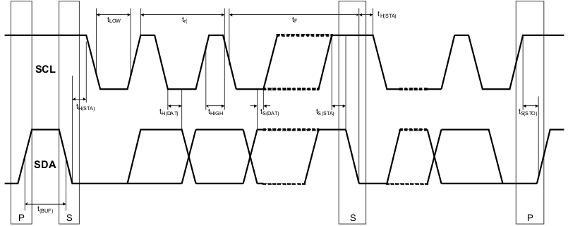 Figure 1. I2C Data Transmission Timing
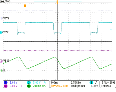
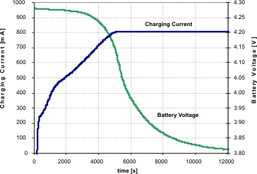
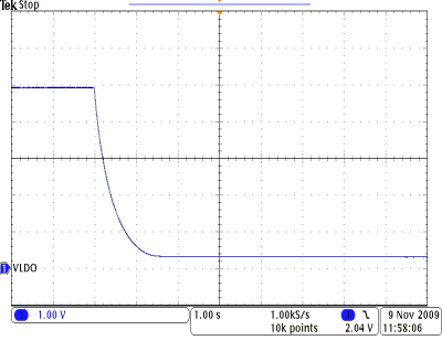
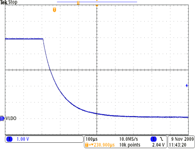
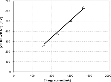 Figure 7. Effective Dropout Voltage
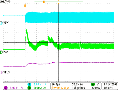
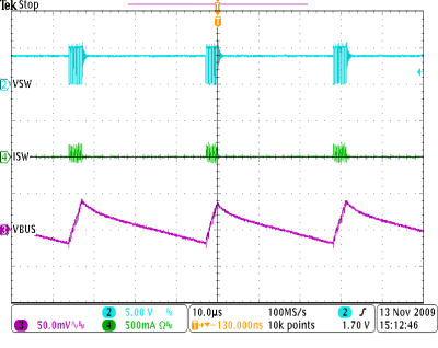
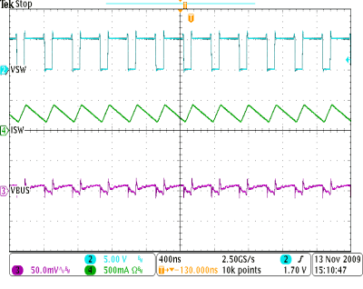
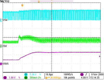
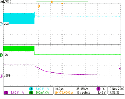
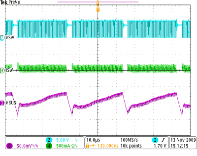
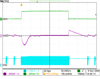
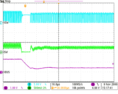
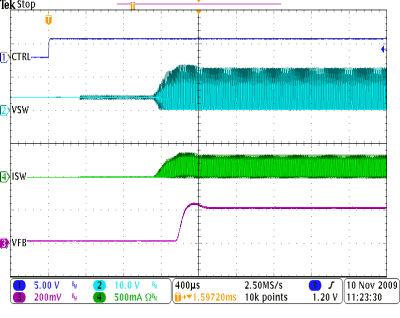
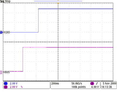 Figure 17. Turnon Delay
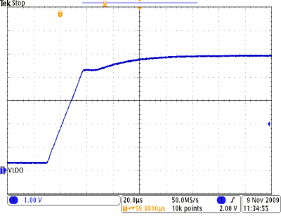
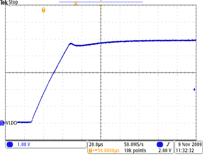
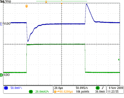
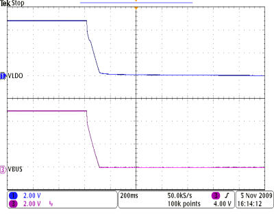 Figure 18. Turnoff Delay
