JAJSLJ7A May   2021  – August 2021 TPS6521855

PRODUCTION DATA  

  1. 特長
  2. アプリケーション
  3. 概要
    1.     4
  4. Revision History
  5. Pin Configuration and Functions
  6. Specifications
    1. 6.1 Absolute Maximum Ratings
    2. 6.2 ESD Ratings
    3. 6.3 Recommended Operating Conditions
    4. 6.4 Thermal Information
    5. 6.5 Electrical Characteristics
    6. 6.6 Timing Requirements
    7. 6.7 Typical Characteristics
  7. Detailed Description
    1. 7.1 Overview
    2. 7.2 Functional Block Diagram
    3. 7.3 Feature Description
      1. 7.3.1 Wake-Up and Power-Up and Power-Down Sequencing
        1. 7.3.1.1  Power-Up Sequencing
        2. 7.3.1.2  Power-Down Sequencing
        3. 7.3.1.3  Strobe 1 and Strobe 2
        4. 7.3.1.4  Supply Voltage Supervisor and Power-Good (PGOOD)
        5. 7.3.1.5  Internal LDO (INT_LDO)
        6. 7.3.1.6  Current Limited Load Switches
          1. 7.3.1.6.1 Load Switch 1 (LS1)
          2. 7.3.1.6.2 Load Switch 2 (LS2)
          3. 7.3.1.6.3 Load Switch 3 (LS3)
        7. 7.3.1.7  LDO1
        8. 7.3.1.8  UVLO
        9. 7.3.1.9  Power-Fail Comparator
        10. 7.3.1.10 DCDC3 and DCDC4 Power-Up Default Selection
        11. 7.3.1.11 I/O Configuration
          1. 7.3.1.11.1 Using GPIO3 as Reset Signal to DCDC1 and DCDC2
        12. 7.3.1.12 Push Button Input (PB)
          1. 7.3.1.12.1 Signaling PB-Low Event on the nWAKEUP Pin
          2. 7.3.1.12.2 Push Button Reset
        13. 7.3.1.13 AC_DET Input (AC_DET)
        14. 7.3.1.14 Interrupt Pin (INT)
        15. 7.3.1.15 I2C Bus Operation
    4. 7.4 Device Functional Modes
      1. 7.4.1 Modes of Operation
      2. 7.4.2 OFF
      3. 7.4.3 ACTIVE
      4. 7.4.4 SUSPEND
      5. 7.4.5 RESET
    5. 7.5 Register Maps
  8. Application and Implementation
    1. 8.1 Application Information
      1. 8.1.1 Applications Without Backup Battery
      2. 8.1.2 Applications Without Battery Backup Supplies
    2. 8.2 Typical Application
      1. 8.2.1 Design Requirements
      2. 8.2.2 Detailed Design Procedure
        1. 8.2.2.1 Output Filter Design
        2. 8.2.2.2 Inductor Selection for Buck Converters
        3. 8.2.2.3 Output Capacitor Selection
      3. 8.2.3 Application Curves
  9. Power Supply Recommendations
  10. 10Layout
    1. 10.1 Layout Guidelines
    2. 10.2 Layout Example
  11. 11Device and Documentation Support
    1. 11.1 Documentation Support
      1. 11.1.1 Related Documentation
    2. 11.2 Receiving Notification of Documentation Updates
    3. 11.3 サポート・リソース
    4. 11.4 Trademarks
    5. 11.5 静電気放電に関する注意事項
    6. 11.6 用語集
  12. 12Mechanical, Packaging, and Orderable Information
    1. 12.1 Package Option Addendum
      1. 12.1.1 Packaging Information
      2. 12.1.2 Tape and Reel Information

パッケージ・オプション

メカニカル・データ(パッケージ|ピン)
サーマルパッド・メカニカル・データ
発注情報

Strobe 1 and Strobe 2

STROBE 1 and STROBE 2 are dedicated to DCDC5 and DCDC6 which are always-on; powered up as soon as the device exits the OFF state, and ON in any other state. STROBE 1 and STROBE 2 options are available only for DCDC5 and DCDC6, not for any other rails.

STROBE 1 and STROBE 2 occur in every power-up sequence, regardless if the rail is already powered up. If the rail is not to be powered up, its respective strobe setting must be set to 0x00.

When a power-down sequence initiates, STROBE 1 and STROBE 2 occur only if the FSEAL bit is 0b. Otherwise, both strobes are omitted and DCDC5 and DCDC6 maintain state.

Note:

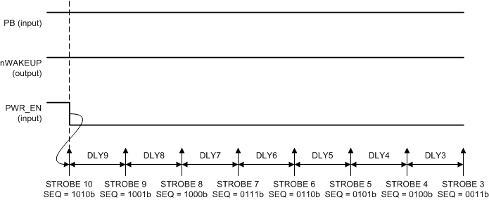
The power-down sequence follows the reverse of the power-up sequence. STROBE2 and STROBE1 are executed only if FSEAL bit is 0b.

GUID-F6FBFCFE-C67F-43FE-BA60-4F4407902710-low.gif Figure 7-4 Power-Down Sequences to OFF State; PWR_EN is Power-Down Event; FSEAL = 0b
GUID-1F0D924D-EBE0-4CEE-B22D-59C60285DBC8-low.gif
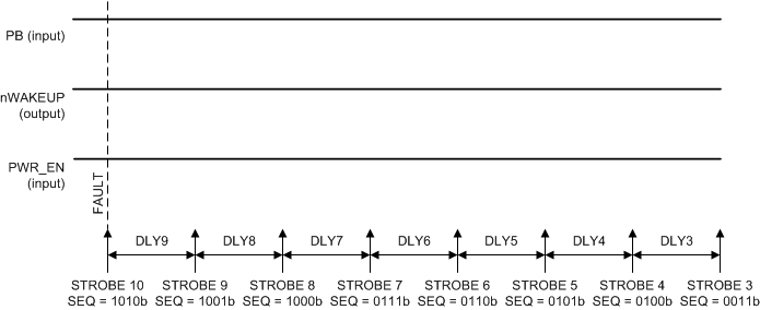
STROBE2 and STROBE1 are not shown.
Figure 7-5 Power-Down Sequences to SUSPEND State; PWR_EN is Power-Down Event; FSEAL = 1b
GUID-E27AD059-1324-4D81-9121-46013E2DA626-low.gif
STROBE2 and STROBE1 are not shown.
Figure 7-6 Power-Down Sequences to RECOVERY State; TSD or UV is Power-Down Event; FSEAL = 1b