JAJSFS2D November   2015  – May 2021 TPS65235

PRODUCTION DATA  

  1. 特長
  2. アプリケーション
  3. 概要
  4. Revision History
  5. Pin Configuration and Functions
  6. Specifications
    1. 6.1 Absolute Maximum Ratings
    2. 6.2 ESD Ratings
    3. 6.3 Recommended Operating Conditions
    4. 6.4 Thermal Information
    5. 6.5 Electrical Characteristics
    6. 6.6 Timing Requirements
    7. 6.7 Typical Characteristics
  7. Detailed Description
    1. 7.1 Overview
    2. 7.2 Functional Block Diagram
    3. 7.3 Feature Description
      1. 7.3.1  Boost Converter
      2. 7.3.2  Linear Regulator and Current Limit
      3. 7.3.3  Boost Converter Current Limit
      4. 7.3.4  Charge Pump
      5. 7.3.5  Slew Rate Control
      6. 7.3.6  Short Circuit Protection, Hiccup and Overtemperature Protection
      7. 7.3.7  Tone Generation
      8. 7.3.8  Tone Detection
      9. 7.3.9  Disable and Enable
      10. 7.3.10 Component Selection
        1. 7.3.10.1 Boost Inductor
        2. 7.3.10.2 Capacitor Selection
        3. 7.3.10.3 Surge Components
        4. 7.3.10.4 Consideration for Boost Filtering and LNB Noise
    4. 7.4 Device Functional Modes
    5. 7.5 Programming
      1. 7.5.1 Serial Interface Description
      2. 7.5.2 TPS65235 I2C Update Sequence
    6. 7.6 Register Maps
      1. 7.6.1 Control Register 1 (address = 0x00H) [reset = 00010000]
      2. 7.6.2 Control Register 2 (address = 0x01H) [reset = 0000101]
      3. 7.6.3 Status Register (address = 0x02H) [reset = x0100000]
  8. Application and Implementation
    1. 8.1 Application Information
    2. 8.2 Typical Application for DiSEqc1.x Support
      1. 8.2.1 Design Requirements
      2. 8.2.2 Detailed Design Procedure
      3. 8.2.3 Application Curves
      4. 8.2.4 Typical Application for DiSEqc2.x Support
        1. 8.2.4.1 Design Requirements
        2. 8.2.4.2 Detailed Design Procedure
        3. 8.2.4.3 Application Curves
  9. Power Supply Recommendations
  10. 10Layout
    1. 10.1 Layout Guidelines
    2. 10.2 Layout Example
  11. 11Device and Documentation Support
    1. 11.1 Receiving Notification of Documentation Updates
    2. 11.2 サポート・リソース
    3. 11.3 Trademarks
    4. 11.4 Electrostatic Discharge Caution
    5. 11.5 Glossary
  12. 12Mechanical, Packaging, and Orderable Information

パッケージ・オプション

メカニカル・データ(パッケージ|ピン)
サーマルパッド・メカニカル・データ
発注情報

TPS65235 I2C Update Sequence

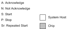
The TPS65235 requires a start condition, a valid I2C address, a register address byte, and a data byte for a single update. After the receipt of each byte, TPS65235 device acknowledges by pulling the SDA line low during the high period of a single clock pulse. TPS65235 performs an update on the falling edge of the LSB byte.

When the TPS65235 is disabled (EN pin tied to ground) the device cannot be updated via the I2C interface.

GUID-551AC695-22DB-45E2-96FB-53BC1AEFF92A-low.gifFigure 7-10 I2C Write Data Format
GUID-682FE2C7-683D-4EE4-B1AB-3F19A751C444-low.gif GUID-C90047FE-EDD2-4B8C-BEE1-41FCE677B86D-low.gifFigure 7-11 I2C Read Data Format