JAJSBH8G June 2010 – February 2018 TPS65251
PRODUCTION DATA.
- 1 特長
- 2 アプリケーション
- 3 概要
- 4 改訂履歴
- 5 概要(続き)
- 6 Pin Configuration and Functions
- 7 Specifications
-
8 Detailed Description
- 8.1 Overview
- 8.2 Functional Block Diagram
- 8.3
Feature Description
- 8.3.1 Adjustable Switching Frequency
- 8.3.2 Synchronization
- 8.3.3 Out-of-Phase Operation
- 8.3.4 Delayed Start-Up
- 8.3.5 Soft-Start Time
- 8.3.6 Adjusting the Output Voltage
- 8.3.7 Input Capacitor
- 8.3.8 Bootstrap Capacitor
- 8.3.9 Error Amplifier
- 8.3.10 Loop Compensation
- 8.3.11 Slope Compensation
- 8.3.12 Powergood
- 8.3.13 Current Limit Protection
- 8.3.14 Overvoltage Transient Protection
- 8.3.15 Thermal Shutdown
- 8.4 Device Functional Modes
-
9 Application and Implementation
- 9.1 Application Information
- 9.2
Typical Application
- 9.2.1 Design Requirements
- 9.2.2
Detailed Design Procedure
- 9.2.2.1 Loop Compensation Circuit
- 9.2.2.2 Selecting the Switching Frequency
- 9.2.2.3 Output Inductor Selection
- 9.2.2.4 Output Capacitor
- 9.2.2.5 Input Capacitor
- 9.2.2.6 Soft-Start Capacitor
- 9.2.2.7 Bootstrap Capacitor Selection
- 9.2.2.8 Adjustable Current Limiting Resistor Selection
- 9.2.2.9 Output Voltage and Feedback Resistors Selection
- 9.2.2.10 Compensation
- 9.2.2.11 3.3-V and 6.5-V LDO Regulators
- 9.2.3 Application Curves
- 10Power Supply Recommendations
- 11Layout
- 12デバイスおよびドキュメントのサポート
- 13メカニカル、パッケージ、および注文情報
パッケージ・オプション
メカニカル・データ(パッケージ|ピン)
- RHA|40
サーマルパッド・メカニカル・データ
- RHA|40
発注情報
7.6 Typical Characteristics
TA = 25°C, VIN = 12 V, fSW = 500 kHz (unless otherwise noted)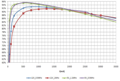
| fSW = 500 kHz, VOUT = 3.3 V, L= 4.7 µH, DCR = 28 mΩ | ||

| CO = 22 µF, VOUT = 3.3 V, L = 4.7 µH | ||
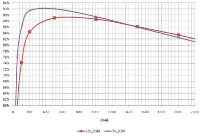
| fSW = 500 kHz, VOUT = 1.8 V, L = 4.7 µH, DCR = 28 mΩ | ||
| (Also Applies to Buck 3) |
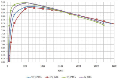
| VOUT = 2.5 V, L = 4.7 µH, DCR = 28 mΩ | ||
| (Also Applies to Buck 2) |
 Figure 9. BUCK1 Line Regulation
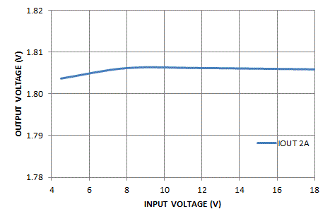 Figure 11. BUCK2 Line Regulation
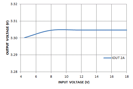 Figure 13. BUCK3 Line Regulation

| fSW = 500 kHz, VOUT = 1.2 V, L = 4.7 µH, DCR = 28 mΩ | ||

| fSW = 500 kHz, VOUT = 3.3 V, L = 4.7 µH, DCR = 28 mΩ | ||
| (Also Applies to Buck 3) |

| VOUT = 2.5 V, L = 4.7 µF | ||

| VOUT = 2.5 V, L = 4.7 µF | ||
 Figure 10. BUCK1 Load Regulation
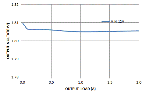 Figure 12. BUCK2 Load Regulation
 Figure 14. BUCK3 Load Regulation