TPS65266 2.7- to 6.5-V Input Voltage, 3-A/2-A/2-A Output Current Triple Synchronous Step-Down Converter
1 Features
- Operating Input Voltage Range 2.7 to 6.5 V
- Feedback Reference Voltage 0.6 V ±1%
- Maximum Continuous Output Current 3 A/2 A/2 A
- Dedicated Enable and Soft Start
- Accurate Start-Up Timing Control With Enable Pins Discharge
- Forced Continuous Current (FCC) Mode at Light Load
- Cycle-by-Cycle Current Limiting With Hiccup Mode Overcurrent Protection
- Adjustable Clock Frequency 250 kHz to 2.4 MHz
- External Clock Synchronization
- Power-Good Indicator
- Overtemperature Protection
2 Applications
- Printer and Scanner
- Digital TV
- Set Top Box
- Home Gateway and Access Point Networks
- Surveillance
3 Description
The TPS65266 incorporates 3 channels of high-efficiency synchronous buck converter for applications operating off the adaptor or battery with input voltage lower than 6.5 V.
The buck DC/DC converter integrates power MOSFETs for optimized power efficiency and reduces external component counts. The peak current mode control simplifies the compensation and fast transient response. High clock frequency allows smaller and low-value inductors and capacitors. External compensation supports optimized loop compensation and fast transient response. In light load condition, the buck converter operates in FCC mode for a reduction in noise susceptibility and RF interference. Cycle-by-cycle overcurrent limiting with hiccup mode limits MOSFET power dissipation in short circuit or overloading fault conditions.
The TPS65266 features a power-good supervisor circuit that monitors all converter outputs. The PGOOD pin is asserted after the output voltages in each channel are in regulation and sequencing is done.
When continuous heavy overload or short circuit increases power dissipation in the buck converter, internal thermal protection circuit shuts off the device to prevent damage. Recovery from a thermal shutdown is automatic after the device has cooled sufficiently.
Device Information(1)
| PART NUMBER | PACKAGE | BODY SIZE (NOM) |
|---|---|---|
| TPS65266 | VQFN (32) | 5.00 mm × 5.00 mm |
- For all available packages, see the orderable addendum at the end of the data sheet.
Simplified Application Schematic

Efficiency vs Output Load

5 Pin Configuration and Functions
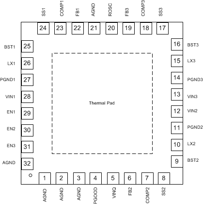
Pin Functions
| PIN | DESCRIPTION | |
|---|---|---|
| NO. | NAME | |
| 1 | AGND | Analog ground pin |
| 2 | AGND | Analog ground pin |
| 3 | AGND | Analog ground pin |
| 4 | PGOOD | An open-drain output; asserts low if output voltage of bucks beyond regulation range due to thermal shutdown, over-current, under-voltage, or ENx low. |
| 5 | VINQ | Input voltage of converter controller and reference power supply bias. TI recommends to connect a 1-µF capacitor from the pin to analog ground and put the capacitor as near as possible to this pin. |
| 6 | FB2 | Feedback Kelvin sensing pin for buck2 output voltage. Connect this pin to buck2 feedback resistor divider. |
| 7 | COMP2 | Error amplifier output and loop compensation pin for buck2. Connect a series resistor and capacitor to compensate the control loop of buck converter 2 with peak current PWM mode. |
| 8 | SS2 | Soft-start and tracking input for buck2 converter. An internal 5.5-µA pullup current source is connected to this pin. The soft-start time of buck2 can be programmed by connecting a capacitor between this pin and ground. |
| 9 | BST2 | Boot strapped supply to the high-side floating gate driver in buck2 converter. Connect a capacitor (47 nF recommended) from BST2 pin to LX2 pin. |
| 10 | LX2 | Switching node connection to the inductor and bootstrap capacitor for buck2 converter. The voltage swing at this pin is from a diode voltage below the ground up to VIN2 voltage. |
| 11 | PGND2 | Power ground connection of buck2. Connect PGND2 pin as close as practical to the (–) terminal of VIN2 input ceramic capacitor. |
| 12 | VIN2 | Input power supply for buck2. Connect VIN2 pin as close as practical to the (+) terminal of an input ceramic capacitor (10 µF suggested). |
| 13 | VIN3 | Input power supply for buck3. Connect VIN3 pin as close as practical to the (+) terminal of an input ceramic capacitor (10 µF suggested). |
| 14 | PGND3 | Power ground connection of buck3. Connect PGND3 pin as close as practical to the (–) terminal of VIN3 input ceramic capacitor. |
| 15 | LX3 | Switching node connection to the inductor and bootstrap capacitor for buck3 converter. The voltage swing at this pin is from a diode voltage below the ground up to VIN3 voltage. |
| 16 | BST3 | Boot strapped supply to the high-side floating gate driver in buck3 converter. Connect a capacitor (47 nF recommended) from BST3 pin to LX3 pin. |
| 17 | SS3 | Soft-start and tracking input for buck3 converter. An internal 5.5-µA pullup current source is connected to this pin. The soft-start time of buck3 can be programmed by connecting a capacitor between this pin and ground. |
| 18 | COMP3 | Error amplifier output and loop compensation pin for buck3. Connect a series resistor and capacitor to compensate the control loop of buck converter 3 with peak current PWM mode. |
| 19 | FB3 | Feedback Kelvin sensing pin for buck3 output voltage. Connect this pin to buck3 feedback resistor divider. |
| 20 | ROSC | Oscillator frequency programmable pin. Connect an external resistor to set the switching frequency. |
| 21 | AGND | Analog ground common to buck controllers and other analog circuits. It must be routed separately from high-current power grounds to the (–) terminal of bypass capacitor of input voltage VINQ. |
| 22 | FB1 | Feedback Kelvin sensing pin for buck1 output voltage. Connect this pin to buck1 feedback resistor divider. |
| 23 | COMP1 | Error amplifier output and loop compensation pin for buck1. Connect a series resistor and capacitor to compensate the control loop of buck converter 1 with peak current PWM mode. |
| 24 | SS1 | Soft-start and tracking input for buck1 converter. An internal 5.5-µA pullup current source is connected to this pin. The soft-start time of buck1 can be programmed by connecting a capacitor between this pin and ground. |
| 25 | BST1 | Boot strapped supply to the high-side floating gate driver in buck1 converter. Connect a capacitor (47 nF recommended) from BST1 pin to LX1 pin. |
| 26 | LX1 | Switching node connection to the inductor and bootstrap capacitor for buck1 converter. The voltage swing at this pin is from a diode voltage below the ground up to VIN1 voltage. |
| 27 | PGND1 | Power ground connection of buck1. Connect PGND1 pin as close as practical to the (–) terminal of VIN1 input ceramic capacitor. |
| 28 | VIN1 | Input power supply for buck1. Connect VIN1 pin as close as practical to the (+) terminal of an input ceramic capacitor (suggest 10 µF). |
| 29 | EN1 | Enable for buck1 converter. Float to enable. Can use this pin to adjust the input undervoltage lockup of buck1 with resistors divider. |
| 30 | EN2 | Enable for buck2 converter. Float to enable. Can use this pin to adjust the input undervoltage lockup of buck2 with resistors divider. |
| 31 | EN3 | Enable for buck3 converter. Float to enable. Can use this pin to adjust the input undervoltage lockup of buck3 with resistors divider. |
| 32 | GND | Ground pin |
| — | Thermal PAD | No electric connection to any signal. Soldered to the ground in PCB for better thermal performance. |