SLVSC85C August   2013  – May 2015 TPS65279

PRODUCTION DATA.  

  1. Features
  2. Applications
  3. Description
  4. Revision History
  5. Description (continued)
  6. Pin Configuration and Functions
  7. Specifications
    1. 7.1 Absolute Maximum Ratings
    2. 7.2 ESD Ratings
    3. 7.3 Recommended Operating Conditions
    4. 7.4 Thermal Information
    5. 7.5 Electrical Characteristics
    6. 7.6 Typical Characteristics
  8. Detailed Description
    1. 8.1 Overview
    2. 8.2 Functional Block Diagram
    3. 8.3 Feature Description
      1. 8.3.1 Enable and Adjusting Undervoltage Lockout (UVLO)
      2. 8.3.2 Adjustable Switching Frequency and Synchronization
        1. 8.3.2.1 Synchronization
      3. 8.3.3 Soft-Start Time
      4. 8.3.4 Out-of-Phase Operation
      5. 8.3.5 Output Overvoltage Protection (OVP)
      6. 8.3.6 Bootstrap Voltage (BOOT) and Low Dropout Operation
      7. 8.3.7 Overcurrent Protection
        1. 8.3.7.1 High-Side MOSFET Overcurrent Protection
        2. 8.3.7.2 Low-Side MOSFET Overcurrent Protection
      8. 8.3.8 Current Sharing Operation
      9. 8.3.9 Thermal Shutdown
    4. 8.4 Device Functional Modes
      1. 8.4.1 CCM Operation Mode
      2. 8.4.2 PSM Operation Mode
      3. 8.4.3 Current Sharing Mode
  9. Application and Implementation
    1. 9.1 Application Information
    2. 9.2 Typical Applications
      1. 9.2.1 Dual Buck Operation Mode Application
        1. 9.2.1.1 Design Requirements
        2. 9.2.1.2 Detailed Design Procedure
          1. 9.2.1.2.1 Adjusting the Output Voltage
          2. 9.2.1.2.2 Adjusting UVLO
          3. 9.2.1.2.3 Adjustable Switching Frequency (Resistor Mode)
          4. 9.2.1.2.4 Output Inductor Selection
          5. 9.2.1.2.5 Output Capacitor Selection
          6. 9.2.1.2.6 Input Capacitor Selection
          7. 9.2.1.2.7 Loop Compensation
        3. 9.2.1.3 Application Curves
      2. 9.2.2 Current Sharing Mode Operation Application
        1. 9.2.2.1 Design Requirements
        2. 9.2.2.2 Detailed Design Procedure
        3. 9.2.2.3 Application Curves
  10. 10Power Supply Recommendations
  11. 11Layout
    1. 11.1 Layout Guidelines
    2. 11.2 Layout Example
  12. 12Device and Documentation Support
    1. 12.1 Community Resources
    2. 12.2 Trademarks
    3. 12.3 Electrostatic Discharge Caution
    4. 12.4 Glossary
  13. 13Mechanical, Packaging, and Orderable Information

パッケージ・オプション

メカニカル・データ(パッケージ|ピン)
サーマルパッド・メカニカル・データ
発注情報

7 Specifications

7.1 Absolute Maximum Ratings

over operating free-air temperature range (unless otherwise noted)(1)
MIN MAX UNIT
Voltage at VIN, PVIN1, PVIN2 –0.3 20 V
Voltage at LX1, LX2 (maximum withstand voltage transient < 20 ns) –4.5 23 V
Voltage at BST1, BST2, referenced to LX1, LX2 pin –0.3 7 V
Voltage at V7V, EN1, EN2, RLIM1, RLIM2, PGOOD1, PGOOD2, MODE, ISHARE, ROSC –0.3 7 V
Voltage at SS1, SS2, FB1, FB2, COMP1, COMP2 –0.3 3.6 V
Voltage at AGND, PGND1, PGND2 –0.3 0.3 V
TJ Operating virtual junction temperature –40 150 °C
Tstg Storage temperature –55 150 °C
(1) Stresses beyond those listed under Absolute Maximum Ratings may cause permanent damage to the device. These are stress ratings only, and functional operation of the device at these or any other conditions beyond those indicated under Recommended Operating Conditions is not implied. Exposure to absolute-maximum-rated conditions for extended periods may affect device reliability.

7.2 ESD Ratings

VALUE UNIT
V(ESD) Electrostatic discharge Human body model (HBM) 2000 V
Charge device model (CDM) 1000

7.3 Recommended Operating Conditions

over operating free-air temperature range (unless otherwise noted)
MIN MAX UNIT
VIN Supply input voltage range 4.5 18 V
IOUT1,
IOUT2
Load current 0 5 A
Vout Output voltage 0.6 9 V
EN Enable voltage 0 6 V
TJ Operating junction temperature –40 125 °C

7.4 Thermal Information

THERMAL METRIC(1) TPS65279 UNIT
DAP (HTSSOP) RHH (VQFN)
32 PINS 36 PINS
RθJA Junction-to-ambient thermal resistance 35 30.8 °C/W
RθJC(top) Junction-to-case (top) thermal resistance 17.7 18.8 °C/W
RθJB Junction-to-board thermal resistance 19 6 °C/W
ψJT Junction-to-top characterization parameter 0.5 0.2 °C/W
ψJB Junction-to-board characterization parameter 18.9 6 °C/W
RθJC(bot) Junction-to-case (bottom) thermal resistance 1.3 0.7 °C/W
(1) For more information about traditional and new thermal metrics, see the Semiconductor and IC Package Thermal Metrics application report, SPRA953.

7.5 Electrical Characteristics

TJ = –40°C to 125°C, VIN = 12 V (unless otherwise noted)
PARAMETER TEST CONDITIONS MIN TYP MAX UNIT
INPUT SUPPLY
VIN Input voltage range VIN1 and VIN2 4.5 18 V
IDDSDN Shutdown supply current EN1 = EN2 = low 10 µA
IDDQ_NSW Switching quiescent current with no load at DCDC output EN1 = EN2 = 3.3 V
With power skip mode, without bucks switching
1.2 mA
IDDQ_SW Switching quiescent current with no load at DCDC output, Buck switching EN1 = EN2 = 3.3 V
With bucks switching
10 mA
UVLO VIN undervoltage lockout Rising VIN 4.25 4.50 V
Falling VIN 3.4 3.75
Hysteresis 0.5
V7V 6.3 V LDO V7V load current = 0 A 6.10 6.3 6.5 V
IOCP_V7V Current limit of V7V LDO 200 mA
ENABLE
VENR Enable threshold Rising 1.21 1.3 V
VENF Enable threshold Falling 1.0 1.17 V
IENR Enable Input current EN = 1 V 3 µA
IENF Enable hysteresis current EN = 1.5 V 3 µA
OSCILLATOR
FSW Switching frequency 200 1600 kHz
ROSC = 100 kΩ (1%) 340 400 460
tSYNC_w Clock sync minimum pulse width 20 ns
VSYNC_HI Clock sync high threshold 2 V
VSYNC_LO Clock sync low threshold 0.8 V
VSYNC_D Clock falling edge to LX rising edge delay 66 ns
FSYNC Clock sync frequency range 200 1600 kHz
BUCK 1, BUCK 2 CONVERTERS
Vref(min) Voltage reference 0 A < IOUT1 < 6 A,
0 A < IOUT2 < 3.5 A
0.594 0.6 0.606 V
VLINEREG Line regulation-DC IOUT = 2 A 0.5 %/V
VLOADREG Load regulation-DC IOUT = (10-90%) x IOUT_max 0.5 %/A
Gm_EA Error amplifier trans-conductance -2 µA < ICOMP < 2 µA 1350 µS
Gm_SRC COMP voltage to inductor current Gm ILX = 0.5 A 10 A/V
ISSx Soft-start pin charging current 6 µA
ILIMIT1 Buck 1 peak inductor current limit RLIM1 = 60.4 kΩ 7.3 A
ILIMIT2 Buck 2 peak inductor current limit RLIM2 = 60.4 kΩ 7.3 A
ILIMITLSx Low side sinking current limit -2.6 A
Rdsonx_HS On resistance of high side FET V7V = 6.3 V 31
Rdsonx_LS On resistance of low side FET VIN = 12 V 23
Tminon Minimum on time 94 ns
VbootUV Boot-LX UVLO 2.1 3 V
Thiccupwait Hiccup wait time 512 cycles
Thiccup_re Hiccup time before re-start 16384 cycles
PGOOD
VPGOOD PGOOD trip levels FB rising to PGOOD high 94%
FB falling to PGOOD low 92.5%
FB rising to PGOOD low 107.5%
FB falliong to PGOOD high 105.5%
THERMAL SHUTDOWN
TTRIP Thermal protection trip point Rising temperature 160  °C
THYST Thermal protection hysteresis 20 °C

7.6 Typical Characteristics

TA = 25°C, VIN = 12 V, ƒSW = 625 kHz (unless otherwise noted)
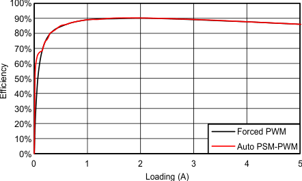
TPS65279 C003_slvsc85.gif
Figure 1. 0.8-V Efficiency
VIN = 12 V, VOUT = 0.8 V
TPS65279 C005_slvsc85.gif
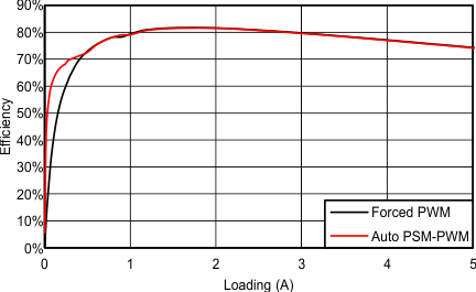
Figure 3. 1.8-V Efficiency
VIN = 12 V, VOUT = 1.8 V
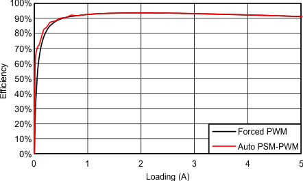
TPS65279 C007_slvsc85.gif
Figure 5. 3.3-V Efficiency
VIN = 12 V, VOUT = 3.3 V
TPS65279 C009_slvsc85.gif
Figure 7. 5-V Efficiency
VIN = 12 V, VOUT = 5 V
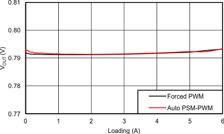
TPS65279 C0011_slvsc85.gif
Figure 9. 0.8-V Load Regulation
VIN = 12 V, VOUT = 0.8 V
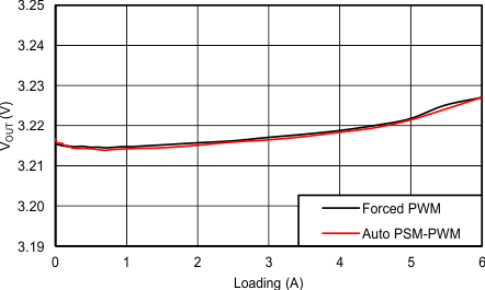
TPS65279 C0013_slvsc85.gif
Figure 11. 3.3-V Load Regulation
VIN = 12 V, VOUT = 3.3 V
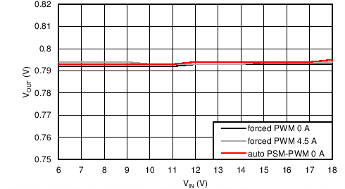
TPS65279 C015_SLVSBW1.png
Figure 13. 0.8-V Line Regulation
VOUT = 0.8 V
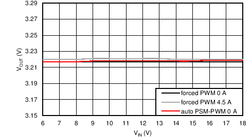
TPS65279 C017_SLVSBW1.png
Figure 15. 3.3-V Line Regulation
VOUT = 3.3 V
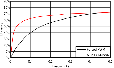
TPS65279 C004_slvsc85.gif
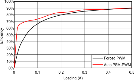
Figure 2. 0.8-V Efficiency, Light Load
VIN = 12 V, VOUT = 0.8 V
TPS65279 C006_slvsc85.gif
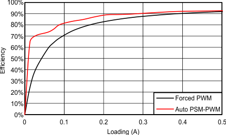
Figure 4. 1.8-V Efficiency, Light Load
VIN = 12 V, VOUT = 1.8 V
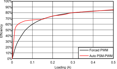
TPS65279 C008_slvsc85.gif
Figure 6. 3.3-V Efficiency, Light Load
VIN = 12 V, VOUT = 3.3 V
TPS65279 C0010_slvsc85.gif
Figure 8. 5-V Efficiency, Light Load
VIN = 12 V, VOUT = 5 V
TPS65279 C0012_slvsc85.gif
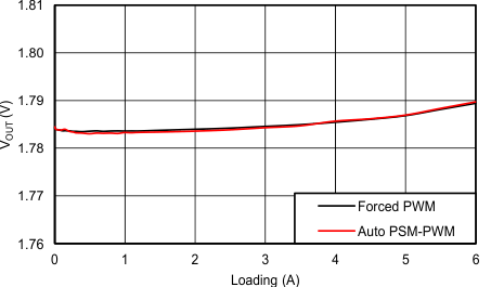
Figure 10. 1.8-V Load Regulation
VIN = 12 V, VOUT = 1.8 V
TPS65279 C0014_slvsc85.gif
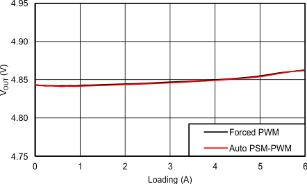
Figure 12. 5-V Load Regulation
VIN = 12 V, VOUT = 5 V
TPS65279 C016_SLVSBW1.png
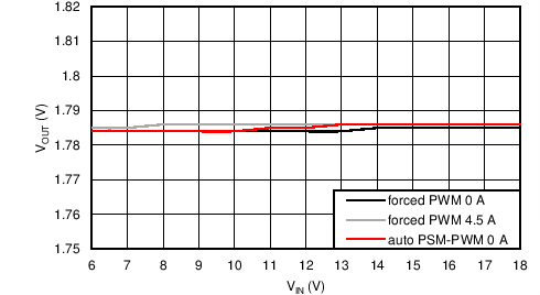
Figure 14. 1.8-V Line Regulation
VOUT = 1.8 V
TPS65279 C018_SLVSBW1.png
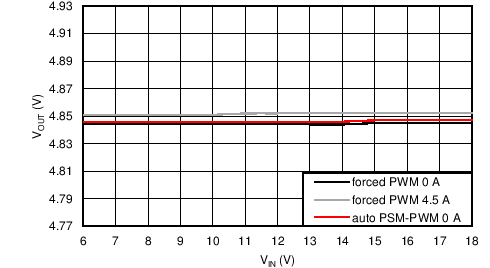
Figure 16. 5-V Line Regulation
VOUT = 5 V