JAJSH01 February   2019 TPS65295

PRODUCTION DATA.  

  1. 特長
  2. アプリケーション
  3. 概要
    1.     代表的なアプリケーション
  4. 改訂履歴
  5. 概要(続き)
  6. Pin Configuration and Functions
    1.     Pin Functions
  7. Specifications
    1. 7.1 Absolute Maximum Ratings
    2. 7.2 ESD Ratings
    3. 7.3 Recommended Operating Conditions
    4. 7.4 Thermal Information
    5. 7.5 Electrical Characteristics
    6. 7.6 Typical Characteristics
  8. Detailed Description
    1. 8.1 Overview
    2. 8.2 Functional Block Diagram
    3. 8.3 Feature Description
      1. 8.3.1 PWM Operation and D-CAP3 Control
      2. 8.3.2 Advanced Eco-mode Control
      3. 8.3.3 Soft Start and Prebiased Soft Start
      4. 8.3.4 Power Good
      5. 8.3.5 Overcurrent Protection and Undervoltage Protection
      6. 8.3.6 Overvoltage Protection
      7. 8.3.7 UVLO Protection
      8. 8.3.8 Output Voltage Discharge
      9. 8.3.9 Thermal Shutdown
    4. 8.4 Device Functional Modes
      1. 8.4.1 Light Load Operation for VDDQ Buck and VPP Buck
      2. 8.4.2 Output State Control
      3. 8.4.3 Output Sequence Control
  9. Application and Implementation
    1. 9.1 Application Information
    2. 9.2 Typical Application
      1. 9.2.1 Design Requirements
      2. 9.2.2 Detailed Design Procedure
        1. 9.2.2.1 External Component Selection
          1. 9.2.2.1.1 Inductor Selection
          2. 9.2.2.1.2 Output Capacitor Selection
          3. 9.2.2.1.3 Input Capacitor Selection
          4. 9.2.2.1.4 Bootstrap Capacitor and Resistor Selection
      3. 9.2.3 Application Curves
  10. 10Power Supply Recommendations
  11. 11Layout
    1. 11.1 Layout Guidelines
    2. 11.2 Layout Example
  12. 12デバイスおよびドキュメントのサポート
    1. 12.1 デバイス・サポート
      1. 12.1.1 デベロッパー・ネットワークの製品に関する免責事項
    2. 12.2 ドキュメントの更新通知を受け取る方法
    3. 12.3 コミュニティ・リソース
    4. 12.4 商標
    5. 12.5 静電気放電に関する注意事項
    6. 12.6 Glossary
  13. 13メカニカル、パッケージ、および注文情報
    1. 13.1 Package Option Addendum
      1. 13.1.1 Packaging Information
      2. 13.1.2 Tape and Reel Information

パッケージ・オプション

メカニカル・データ(パッケージ|ピン)
サーマルパッド・メカニカル・データ
発注情報

Output Sequence Control

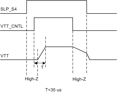
There are specific sequencing requirements for the DDR4 VDDQ and VPP rails. The TPS65295 follows the DDR4 power rail sequence requirements as shown in Figure 29 and Figure 30. VPP is greater than VDDQ at all times during ramp up, operating, and ramp down. The VTT output ramp and stable within 35 µs after VTT_CNTL asserted.
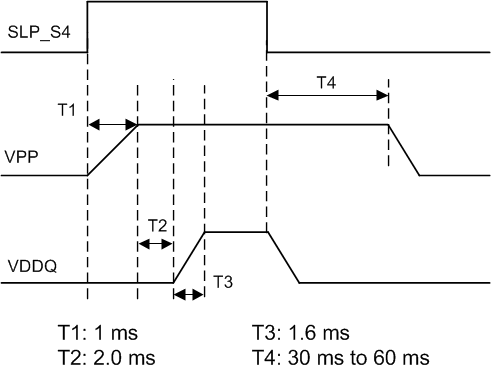
TPS65295 timing-v02-slvsek000.gifFigure 29. Power Sequence, VPP and VDDQ vs SLP_S4
TPS65295 timing-02-slvsek0.gifFigure 30. Power Sequence, VTT vs VTT_CNTL