SLVSBB6F March 2012 – July 2015 TPS65300-Q1
PRODUCTION DATA.
- 1 Features
- 2 Applications
- 3 Description
- 4 Revision History
- 5 Pin Configuration and Functions
-
6 Specifications
- 6.1 Absolute Maximum Ratings
- 6.2 ESD Ratings
- 6.3 Recommended Operating Conditions
- 6.4 Thermal Information
- 6.5 DC Characteristics
- 6.6 Timing Requirements
- 6.7 Switching Characteristics
- 6.8 Typical Characteristics
- 6.9 5-V Linear Regulator (5VO)
- 6.10 3.3-V Linear Regulator Controller (3.3VO)
- 6.11 1.234-V Linear Regulator Controller (1.2VO)
- 7 Detailed Description
-
8 Application and Implementation
- 8.1 Application Information
- 8.2
Typical Application
- 8.2.1 Design Requirements
- 8.2.2 Detailed Design Procedure
- 8.2.3 Application Curves
- 9 Power Supply Recommendations
- 10Layout
- 11Device and Documentation Support
- 12Mechanical, Packaging, and Orderable Information
パッケージ・オプション
メカニカル・データ(パッケージ|ピン)
サーマルパッド・メカニカル・データ
- PWP|24
発注情報
8 Application and Implementation
NOTE
Information in the following applications sections is not part of the TI component specification, and TI does not warrant its accuracy or completeness. TI’s customers are responsible for determining suitability of components for their purposes. Customers should validate and test their design implementation to confirm system functionality.
8.1 Application Information
This section is a starting point and theoretical representation of the values to be used for the application, further optimization of the components derived may be required to improve the performance of the device.
8.2 Typical Application
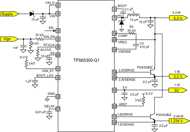
S1: MBRS310T3 (ON Semiconductors) or SS3H10 (Vishay)
S2: B240A, SS16 (Vishay)
External BJT: PBSS302NZ (NXP)
8.2.1 Design Requirements
For this design example, use the parameters listed in Table 1.
Table 1. Switching Regulator Requirements
| Parameter | Requirement |
|---|---|
| Input voltage, VI | 6.5 V to 27 V, typical 14 V |
| Output voltage, 5.3 V | 5.3 VO ±2% at 5.3 W |
| Maximum output current I5.3V_max | 1 A |
| Minimum output current I5.3V_min | 0.01 A |
| Transient response 0.01A to 0.8 A | 5% |
| Reset threshold | 90% of output voltage |
| 5V | 5VO at 1 W |
| 3.3V | 3.3VO at 1 W |
| 1.234V | 1.234VO at 0.5 W |
| Switching frequency fSW | 2.5 MHz |
| Overvoltage threshold | 106% of output voltage |
| Undervoltage threshold | 95% of output voltage |
8.2.2 Detailed Design Procedure
The following design procedure provides typical application procedures as well as the details of a switching regulator design using the requirements listed in Table 1.
8.2.2.1 Duty Cycle
Use Equation 7 to calculate the duty cycle.

where
- VO = Output voltage
- VI = Input voltage
8.2.2.2 Output Inductor Selection (L)
The minimum inductor value is calculated using the coefficient KIND that represents the amount of inductor ripple current relative to the maximum output current. The inductor ripple current is filtered by the output capacitor, and so the typical range of this ripple current is in the range of KIND = 0.2 to 0.3, depending on the ESR and the ripple-current rating of the output capacitor.
For this design example, use Equation 8 to calculate the inductor ripple current

where
- IO = Output current
Benefits of Low Inductor Value
- Low inductor value gives high di/dt, which allows for fewer output capacitors for good load transient response.
- Gives higher saturation current for the core due to fewer turns
- Fewer turns yields low DCR and therefore less dc inductor losses in the windings.
- High di/dt provides faster response to load steps.
Benefits of High Inductor Value
- Low ripple current leads to lower conduction losses in MOSFETs
- Low ripple; means lower RMS ripple current for capacitors
- Low ripple; yields low ac inductor losses in the core (flux) and windings (skin effect)
- Low ripple; gives continuous inductor current flow over a wide load range
For this design example a value of 10 µH was selected because of variations in temperature and manufacture. Use Equation 9 to find the value of LMin.

where
- fSW is the regulator switching frequency
- IRipple = Allowable ripple current in the inductor, typically ±20% of maximum output load IO
For this design example, use Equation 10 to calculate the inductor peak current.

8.2.2.3 Output Capacitor Selection (CO)
The selection of the output capacitor determines several parameters in the operation of the converter, the modulator pole, the voltage droop on the out capacitor, and the output ripple.
During a load step from no load to full load or changes in the input voltage, the output capacitor must hold up the output voltage above a certain level for a specified time and not issue a reset until the main regulator control loop responds to the change. The capacitance value determines the modulator pole and the roll-off frequency due to because of the LC output-filter double pole—the output ripple voltage is a product of the output capacitor ESR and ripple current.
Use Equation 11 to calculate the minimum capacitance required to maintain desired output voltage during a high-to-low load transition and prevent overshoot.

where
- IO-max is maximum output current
- IO-min is minimum output current
- The difference between the output current, maximum to minimum, is the worst-case load step in the system.
- VO-max is maximum tolerance of regulated output voltage
- VO-min is the minimum tolerance of regulated output voltage
Use Equation 12 to calculate the output capacitor root-mean-square (RMS) ripple current IO_RMS. This is to prevent excess heating or failure due to high ripple currents.
This parameter is sometimes specified by the manufacturer. Therfore, because of variations in temperature and manufacture, use a 10-µF capacitor with a voltage rating greater than the maximum 10-V output.

8.2.2.4 External Schottky Diode (D)
The TPS65300-Q1 device requires an external ultrafast Schottky diode with fast reverse-recovery time connected between the PH and power ground pins. The diode conducts the output current during the off-state of the internal power switch. This diode must have a reverse breakdown higher than the maximum input voltage of the application. A Schottky diode is selected for lower forward voltage. The Schottky diode is selected based on the appropriate power rating, which factors in the DC-conduction losses and the AC losses because of the high switching frequencies. The power dissipation PD is calculated with Equation 13.

where
- VFD = forward conducting voltage of Schottky diode
- CJ = junction capacitance of the Schottky diode
8.2.2.5 Input Capacitor (CI)
The TPS65300-Q1 device requires an input ceramic decoupling capacitor type X5R or X7R and bulk capacitance to minimize input ripple voltage. The DC voltage rating of this input capacitance must be greater than the maximum input voltage. The capacitor must have an input ripple-current rating higher than the maximum input ripple current of the converter for the application. The input capacitors for power regulators are selected to have reasonable capacitance-to-volume ratio and to be fairly stable over temperature. The value of the input capacitance is based on the input voltage desired (∆VI).
Use Equation 14 to calculate the input capacitance.

Use Equation 15 to calculate the input-capacitor root-mean-square (RMS) ripple current II_RMS.
Because of variations in temperature and manufacture, use a 10-µF capacitor with a voltage rating greater than the maximum 45-V transient.

8.2.2.6 Loop Compensation
The double pole is because of the output-filter components inductor and capacitor. The calculations for the following equations use values taken from Figure 14.
8.2.2.7 Loop-Control Frequency Compensation
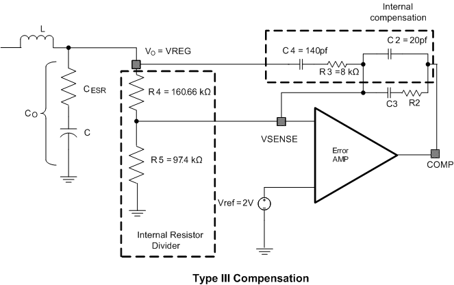 Figure 14. Loop-Control Frequency Compensation
8.2.2.7.1 Type III Compensation
fCO = fSW × 0.1 (the cutoff frequency when the gain is 1 is called the unity-gain frequency).
fCO is typically 1/5 to 1/10 of the switching frequency double-pole frequency response due to the LC output filter. The LC output filter gives a double pole, which has a –180° phase shift.
Make the two zeroes close to the double pole (LC), for example, fZ1 ≈ fZ2 ≈ 1/2π(LCOUT)1/2.
- Make the first zero below the filter double pole (approximately 50% to 75% of fLC)
- Make the second zero at the filter double pole (fLC)
- Make the first pole at the ESR frequency (fESR)
- Make the second pole at 0.5 the switching frequency
Make the two poles above the crossover frequency fCO.
The following compensation components are integrated in the device with the following typical values. Guidelines for compensation components:
R3 = 8 kΩ, C4 = 140 pF, C2 = 20 pF
Use Equation 16 to calculate the double pole to calculate the output filter components LC.

The ESR of the output capacitor C gives a zero that has a 90° phase shift. The ESR of the output capacitor must be in the range of 1 mΩ to 100 mΩ. Use Equation 17 to calculate the value of fESR.

8.2.2.7.2 PWM Modulator Gain K

where
- Vramp = VI / 10, VI = Input operating voltage
8.2.2.7.3 Resistor Values
In this design example, select a value of 97.4 k Ω for R5 and use Equation 19 to calculate the value of R4.

where
- Vref = 2 V
Use Equation 20 to calculate the value of R2 for this design example.

Calculate C3 based on placing a zero at 50% to 75% of the output-filter double-pole frequency (below set at 50%).
For this design example, use Equation 21 to calculate the value of C3 as 80 pF.

8.2.2.7.4 Gain of Amplifier

8.2.2.7.5 Poles and Zero Frequencies
The following equations were used in this design example:
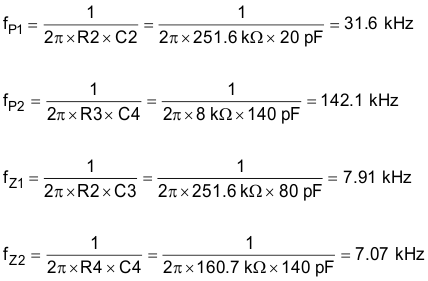
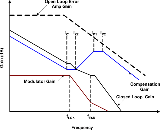 Figure 15. Typical Gain Versus Frequency
8.2.2.8 Power Dissipation
8.2.2.8.1 Switch-Mode Power-Supply Losses
The power dissipation losses are applicable for continuous-conduction mode operation (CCM).
- Conduction losses
- IO = Output current
- VO = VREG = Output voltage
- VI = Input voltage
- fSW = Switching frequency
- Switching losses
- tr = FET switching rise time (tr max = 20 ns)
- tf = FET switching fall time (tf max = 20 ns)
- Gate drive losses
- Vdrive = FET gate-drive voltage (typically Vdrive = 6 V and Vdrive max = 8 V)
- Qg = 1 × 10⁻⁹ (nC) (typical)
- Supply losses
where
where
where
Therefore:
Therefore, for this design, the following equations were used:
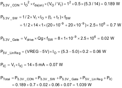
For given operating ambient temperature TA
where
- TJ = Junction temperature in °C
- TA = Ambient temperature in °C
- PTotal = Total power dissipation (watts)
For a given max junction temperature TJ-Max = 150°C
where
- TA-Max = Maximum ambient temperature in °C
- TJ-Max = Maximum junction temperature in °C
- Rth = Thermal resistance of package in (°C/W)
Other factors not included in the foregoing information which affect the overall efficiency and power losses are
- Inductor AC and DC losses
- Trace resistance and losses associated with the copper trace routing connection
- Schottky diode
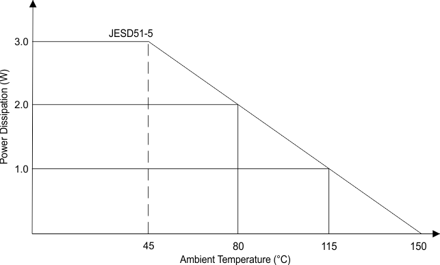 Figure 16. Power Dissipation Derating Profile, 24-Pin PWP Package With Thermal Pad
