SLVSC10C October 2013 – April 2016 TPS65301-Q1
PRODUCTION DATA.
- 1 Features
- 2 Applications
- 3 Description
- 4 Revision History
- 5 Pin Configuration and Functions
- 6 Specifications
- 7 Detailed Description
-
8 Application and Implementation
- 8.1 Application Information
- 8.2
Typical Application
- 8.2.1 Design Requirements
- 8.2.2 Detailed Design Procedure
- 8.2.3 Application Curves
- 9 Power Supply Recommendations
- 10Layout
- 11Device and Documentation Support
- 12Mechanical, Packaging, and Orderable Information
パッケージ・オプション
メカニカル・データ(パッケージ|ピン)
- PWP|24
サーマルパッド・メカニカル・データ
- PWP|24
発注情報
1 Features
- Qualified for Automotive Applications
- AEC-Q100 Qualified with the Following Results
- Device Temperature Grade 1: –40°C to 125°C Ambient Operating Temperature Range
- Device HBM ESD Classification Level H2
- Device CDM ESD Classification Level C4B
- Input VIN Range 5.6 V to 40 V, With Transients up to 45 V
- 5.45-V Switch-Mode Regulator With Integrated High-Side Switch
- Recommended Switch-Mode Frequency Range 2 MHz to 3 MHz
- Overcurrent Protection and 1.2-A Peak Switch Current
- One Linear Regulator 5 V ±2%
- Two Linear Regulator Controllers With 3.3-V and 1.2 V ±2%
- Status Indicator Output of IGN_EN Input
- Soft Start on IGN_EN and EN
- External Clock Input for Synchronization
- Programmable Power-On-Reset Delay, Reset-Function Filter Timer for Fast Negative Transients
- Voltage Supervisor for the Following Supplies
- Thermally Enhanced 24-Pin HTSSOP or 24-Pin VQFN Package
- Protected 5-V Sensor Supply Output, Which Tracks 3.3-V Supply
2 Applications
- Power Supply for TMS570 Microcontrollers
- Power Supply for C28XXX DSP
- General-Purpose Power Supply for Automotive Applications
3 Description
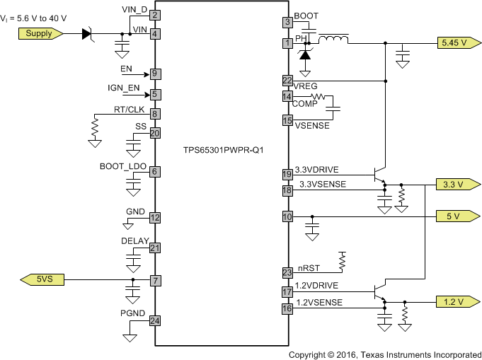
The TPS65301-Q1 power supply is a combination of a single switch-mode buck power supply and three linear regulators. This is a monolithic high-voltage switching regulator with an integrated 1.2-A peak current switch, 45-V power MOSFET, one low-voltage linear regulator, two voltage-regulator controllers and a protected sensor supply.
The device has a voltage supervisor which monitors the output of the switch-mode power supply, the 3.3-V linear regulator, and the 1.2-V linear regulator. An external timing capacitor is used to set the power-on delay and the release of the reset output nRST. This reset output is also used to indicate if the switch-mode supply, the 3.3-V linear regulator supply, or the 1.2-V linear regulator supply is outside the set limits. The protected sensor supply 5VS tracks the 3.3-V linear regulator within the specified limits.
The TPS65301-Q1 device has a switching frequency range from 2 MHz to 3 MHz, allowing the use of low-profile inductors and low-value input and output ceramic capacitors. External loop compensation gives the user the flexibility to optimize the converter response for the appropriate operating conditions.
This device has built-in protection features such as soft start on IGN_EN ON or enables cycle, pulse-by-pulse current limit, thermal sensing, and shutdown due to excessive power dissipation.
Device Information(1)
| PART NUMBER | PACKAGE | BODY SIZE (NOM) |
|---|---|---|
| TPS65301-Q1 | HTSSOP (24) | 7.80 mm × 4.40 mm |
| VQFN (24) | 5.00 mm × 4.00 mm |
- For all available packages, see the orderable addendum at the end of the data sheet.
Typical Application Schematic

4 Revision History
Changes from B Revision (December 2013) to C Revision
- Changed the Features section Go
- Changed the minimum VIN value from 5.75 to 5.6 in the Features and Power Supply Recommendations sections Go
- Added Pin Configuration and Functions section, ESD Ratings table, Feature Description section, Device Functional Modes, Application and Implementation section, Power Supply Recommendations section, Layout section, Device and Documentation Support section, and Mechanical, Packaging, and Orderable Information sectionGo
- Updated the pin types and descriptions in the Pin Functions tableGo
- Changed the maximum PH buck regulator voltage in the Absolute Maximum Ratings table Go
- Moved the TA value from the Recommended Operating Conditions table to the Absolute Maximum Ratings table Go
- Changed DC CHARACTERISTICS condition statement from TJ = –40°C to 150°C to TJ-Max = 150°CGo
Changes from A Revision (November 2013) to B Revision
- Changed the Operating Junction Temperature Range from –40°C to 150°C to up to 150°C in the FEATURES listGo
- Changed DC CHARACTERISTICS condition statement from TJ = –40°C to 150°C to TJ-Max = 150°CGo
- Added Output Voltage vs Output Current graph to TYPICAL CHARACTERISTICS sectionGo
- Changed Y-axis name from Current (mA) to Efficiency in the EFFICIENCY vs OUTPUT CURRENT ON VREG graph in the TYPICAL CHARACTERISTICS sectionGo
Changes from * Revision (October 2013) to A Revision
- Changed document status from Product Preview to Production DataGo
- Changed min value for VIL in the DC CHARACTERISTICS table from 2 to 2.2Go
- Deleted the 5VS oft-start time, TSS, parameter from the DC CHARACTERISTICS tableGo
- Changed the min, typ, and max values for the nRST parameter for VREG output from 0.87, 0.9, and 0.93 to 0.845, 0.875, and 0.905 respectivelyGo