SLVSAY9F December 2012 – March 2016 TPS65320-Q1
PRODUCTION DATA.
- 1 Features
- 2 Applications
- 3 Description
- 4 Revision History
- 5 Pin Configuration and Functions
- 6 Specifications
-
7 Detailed Description
- 7.1 Overview
- 7.2 Functional Block Diagram
- 7.3
Feature Description
- 7.3.1
Buck Regulator
- 7.3.1.1 Fixed-Frequency PWM Control
- 7.3.1.2 Slope Compensation Output
- 7.3.1.3 Pulse-Skip Eco-mode™ Control Scheme
- 7.3.1.4 Dropout Operation and Bootstrap Voltage (BOOT)
- 7.3.1.5 Error Amplifier
- 7.3.1.6 Voltage Reference
- 7.3.1.7 Adjusting the Output Voltage
- 7.3.1.8 Soft-Start and Tracking Pin (SS/TR)
- 7.3.1.9 Overload Recovery Circuit
- 7.3.1.10 Constant Switching Frequency and Timing Resistor (RT/CLK Pin)
- 7.3.1.11 Overcurrent Protection and Frequency Shift
- 7.3.1.12 Selecting the Switching Frequency
- 7.3.1.13 How to Interface to RT/CLK Pin
- 7.3.1.14 Overvoltage Transient Protection
- 7.3.1.15 Thermal Shutdown
- 7.3.1.16 Small-Signal Model for Loop Response
- 7.3.1.17 Simple Small-Signal Model for Peak-Current Mode Control
- 7.3.1.18 Small-Signal Model for Frequency Compensation
- 7.3.2 LDO Regulator
- 7.3.3 Enable and Undervoltage Lockout
- 7.3.1
Buck Regulator
- 7.4 Device Functional Modes
-
8 Application and Implementation
- 8.1 Application Information
- 8.2
Typical Applications
- 8.2.1
2.2-MHz Switching Frequency, 9-V to 16-V Input, 5-V Output Buck Regulator, 3.3-V Output LDO Regulator
- 8.2.1.1 Design Requirements
- 8.2.1.2
Detailed Design Procedure
- 8.2.1.2.1 Switching Frequency Selection for the Buck Regulator
- 8.2.1.2.2 Output Inductor Selection for the Buck Regulator
- 8.2.1.2.3 Output Capacitor Selection for the Buck Regulator
- 8.2.1.2.4 Catch Diode Selection for the Buck Regulator
- 8.2.1.2.5 Input Capacitor Selection for the Buck Regulator
- 8.2.1.2.6 Soft-Start Capacitor Selection for the Buck Regulator
- 8.2.1.2.7 Bootstrap Capacitor Selection for the Buck Regulator
- 8.2.1.2.8 Output Voltage and Feedback Resistor Selection for the Buck Regulator
- 8.2.1.2.9 Frequency Compensation Selection for the Buck Regulator
- 8.2.1.2.10 LDO Regulator
- 8.2.1.2.11 Power Dissipation
- 8.2.1.2.12 Power Dissipation Losses of the LDO Regulator
- 8.2.1.2.13 Total Device Power Dissipation Losses and Junction Temperature
- 8.2.1.3 Application Curves
- 8.2.2 Design Example With 500-kHz Switching Frequency
- 8.2.1
2.2-MHz Switching Frequency, 9-V to 16-V Input, 5-V Output Buck Regulator, 3.3-V Output LDO Regulator
- 9 Power Supply Recommendations
- 10Layout
- 11Device and Documentation Support
- 12Mechanical, Packaging, and Orderable Information
パッケージ・オプション
デバイスごとのパッケージ図は、PDF版データシートをご参照ください。
メカニカル・データ(パッケージ|ピン)
- PWP|14
サーマルパッド・メカニカル・データ
- PWP|14
発注情報
1 Features
- Qualified for Automotive Applications
- AEC-Q100 Qualified With the Following Results:
- Device Temperature Grade 1: –40°C to +125°C Ambient Operating Temperature
- Device HBM ESD Classification Level 2
- Device CDM ESD Classification Level C4B
- One High-VIN Step-Down Converter
- 3.6- to 40-V Input Range
- 250-mΩ High-Side MOSFET
- 3.2-A Maximum Load Current, 1.1- to 20-V Output Adjustable
- 100-kHz to 2.5-MHz Adjustable Switch-Mode Frequency
- Less Than 140-µA Operating Quiescent Current
- One Low-Dropout Voltage Regulator (LDO)
- 280-mA Current Capability With 28-μA (Typical) Operating Quiescent Current in No-Load Condition
- Input Supply Auto-Source to Balance Efficiency and Low Standby Current
- Power-Good Output (Push-Pull)
- Low-Dropout Voltage of 300 mV at IOUT = 200 mA (Typical)
- Overcurrent Protection for Both Regulators
- Overtemperature Protection
- 14-Pin HTSSOP Package With PowerPAD™ Package
2 Applications
3 Description
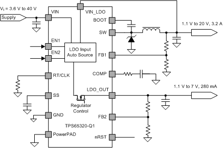
The TPS65320-Q1 device is a combination of a 40-V, 3.2-A, DC-DC step-down converter and a low-dropout (LDO) regulator. The DC-DC step-down converter, referred to as the buck regulator, has an integrated high-side MOSFET. The LDO regulator also has an integrated MOSFET and a low-input supply current of 28-μA (typical) in a no-load condition. Furthermore, the LDO regulator has an active-low, push-pull reset output pin. To reduce heat, the input supply of the LDO regulator can auto-source from the input voltage to the output of the buck regulator. The low-voltage tracking feature can eliminate the need to use a boost converter during cold-crank conditions.
The buck regulator has a switching frequency range from 100 kHz to 2.5 MHz that provides a flexible design to fix system requirements. The external loop compensation allows for optimization of the converter response for the appropriate operating conditions. A low-ripple pulse-skip mode reduces the no-load input supply current to less than 140 μA.
The device has built-in protection features such as soft start, current limit, thermal sensing, and shutdown because of excessive power dissipation. Furthermore, the device has an internal undervoltage-lockout (UVLO) function that turns off the device at a too-low supply voltage.
Device Information(1)
| PART NUMBER | PACKAGE | BODY SIZE (NOM) |
|---|---|---|
| TPS65320-Q1 | HTSSOP (14) | 5.00 mm × 4.40 mm |
Typical Application Schematic

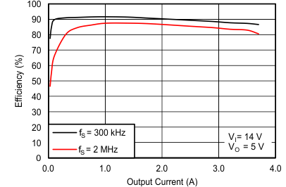
Buck Efficiency Versus Output Current
