JAJSD95A July 2016 – May 2017 TPS65381A-Q1
PRODUCTION DATA.
- 1 デバイスの概要
- 2 改訂履歴
- 3 Pin Configuration and Functions
- 4 Specifications
-
5 Detailed Description
- 5.1 Overview
- 5.2 Functional Block Diagram
- 5.3 Feature Description
- 5.4
Device Functional Modes
- 5.4.1 Power-Up and Power-Down Behavior
- 5.4.2 Safety Functions and Diagnostics Overview
- 5.4.3 Voltage Monitor (VMON)
- 5.4.4 TPS65381A-Q1 Internal Error Signals
- 5.4.5 Loss-of-Clock Monitor (LCMON)
- 5.4.6 Analog Built-In Self-Test (ABIST)
- 5.4.7 Logic Built-In Self-Test (LBIST)
- 5.4.8 Junction Temperature Monitoring and Current Limiting
- 5.4.9 Diagnostic MUX and Diagnostic Output Pin (DIAG_OUT)
- 5.4.10 Watchdog Timer (WD)
- 5.4.11 Watchdog Fail Counter, Status, and Fail Event
- 5.4.12 Watchdog Sequence
- 5.4.13 MCU to Watchdog Synchronization
- 5.4.14 Trigger Mode (Default Mode)
- 5.4.15 Q&A Mode
- 5.4.16 MCU Error Signal Monitor (MCU ESM)
- 5.4.17 Device Configuration Register Protection
- 5.4.18 Enable and Reset Driver Circuit
- 5.4.19 Device Operating States
- 5.4.20 STANDBY State
- 5.4.21 RESET State
- 5.4.22 DIAGNOSTIC State
- 5.4.23 ACTIVE State
- 5.4.24 SAFE State
- 5.4.25 State Transition Priorities
- 5.4.26 Power on Reset (NPOR)
- 5.5
Register Maps
- 5.5.1 Serial Peripheral Interface (SPI)
- 5.5.2 SPI Register Write Access Lock (SW_LOCK command)
- 5.5.3 SPI Registers (SPI Mapped Response)
- 5.5.4
Device Safety Status and Control Registers
- 5.5.4.1 VMON_STAT_1 Register
- 5.5.4.2 VMON_STAT_2 Register
- 5.5.4.3 SAFETY_STAT_1 Register
- 5.5.4.4 SAFETY_STAT_2 Register
- 5.5.4.5 SAFETY_STAT_3 Register
- 5.5.4.6 SAFETY_STAT_4 Register
- 5.5.4.7 SAFETY_STAT_5 Register
- 5.5.4.8 SAFETY_ERR_CFG Register
- 5.5.4.9 SAFETY_BIST_CTRL Register
- 5.5.4.10 SAFETY_CHECK_CTRL Register
- 5.5.4.11 SAFETY_FUNC_CFG Register
- 5.5.4.12 SAFETY_ERR_STAT Register
- 5.5.4.13 SAFETY_ERR_PWM_H Register
- 5.5.4.14 SAFETY_ERR_PWM_L Register
- 5.5.4.15 SAFETY_PWD_THR_CFG Register
- 5.5.4.16 SAFETY_CFG_CRC Register
- 5.5.4.17 Diagnostics
- 5.5.5 Watchdog Timer
- 5.5.6 Sensor Supply
-
6 Application and Implementation
- 6.1 Application Information
- 6.2
Typical Application
- 6.2.1 Design Requirements
- 6.2.2
Detailed Design Procedure
- 6.2.2.1 VDD6 Preregulator
- 6.2.2.2 VDD1 Linear Controller
- 6.2.2.3 VSOUT1 Tracking Linear Regulator, Configured to Track VDD5
- 6.2.2.4 Alternative Use for VSOUT1 Tracking Linear Regulator, Configured for 6-V Output Tracking VDD3/5 In 3.3-V Mode
- 6.2.2.5 Alternative Use for VSOUT1 Tracking Linear Regulator, Configured for 9-V Output Tracking to 5-V Input from VDD5
- 6.2.2.6 Alternative Use for VSOUT1 Tracking Linear Regulator, Configured in Non-tracking Mode Providing a 4.5-V Output
- 6.2.3 Application Curves
- 6.3 System Examples
- 7 Power Supply Recommendations
- 8 Layout
- 9 デバイスおよびドキュメントのサポート
- 10メカニカル、パッケージ、および注文情報
パッケージ・オプション
メカニカル・データ(パッケージ|ピン)
- DAP|32
サーマルパッド・メカニカル・データ
- DAP|32
発注情報
6 Application and Implementation
NOTE
Information in the following applications sections is not part of the TI component specification, and TI does not warrant its accuracy or completeness. TI’s customers are responsible for determining suitability of components for their purposes. Customers should validate and test their design implementation to confirm system functionality.
6.1 Application Information
The TPS65381A-Q1 device is a multirail power supply including one buck preregulator, one linear controller, one 5-V linear regulator, one programmable 3.3-V or 5-V linear regulator, and one linear tracking regulator with protection against short to battery and ground. The device has many diagnostic and monitoring functions. This device provides a power-management basis for many different applications.
6.2 Typical Application
The following design requirements and design procedure are an example of how to select component values for the TPS65381A-Q1 device for a typical application. Because many of the regulators are adjustable, the equations should be used to calculate the component values for the specific application. For additional reference, also refer to the design checklist and application notes listed in Section 9.1.1.
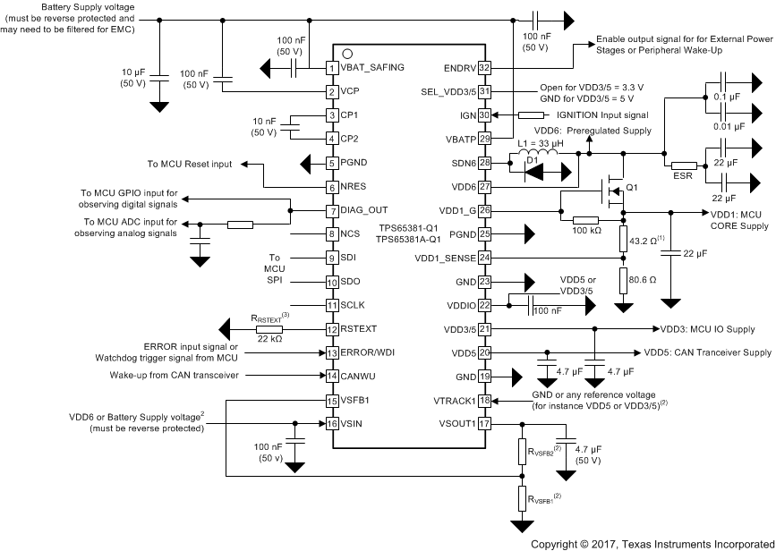
- Q1: BUK9213-30A
- D1: Vishay SS3H09/10, OnSemi MBRS340T3
- D2: ROHM UDZSTE-176.2B
- L1: TDK CLF10060NIT-330M-D or COILCRAFT MSS1246T-333ML
NOTE:
- 43.2 Ω for 1.23-V output voltage (Recommended for TI TMS570 MCU). Change this resistor to obtain different VDD1 output voltage, VDD1_SENSE = 800 mV. The tolerance of the resistors in this resistor divider will impact VDD1 regulation and voltage monitoring tolerance. Resistors with 0.1% tolerance are recommended.
- RVSFB1 and RVSFB2 configure the VSOUT1 voltage
- Pin 16 (VSIN) to be connected either to pin 27 (VDD6) for VSOUT1 ≤ 5 V or to pin 29 (VBATP) for 5 V < VSOUT1 < 9.5 V
- Pin 18 (VTRACK1) to be connected to GND for non-tracking mode, or a reference voltage (for example VDD5 or VDD3/5) for tracking mode.
- The tolerance of the resistors in this resistor divider will impact VSOUT1 regulation and voltage monitoring tolerance. Resistors with 0.1% tolerance are recommended.
- See Section 5.3.5 for details.
- RRSEXT configures the Reset Extension time. See the Reset and Enable outputs section of Section 4.5
6.2.1 Design Requirements
While selecting capacitors for the application consider the following characteristics:
- The effective capacitance at the operating voltage must be used when selecting the proper capacitor. Capacitors derate with operating voltage, sometimes as much as 70%. Therefore the capacitance of the circuit could be outside of the specified value for the capacitor as listed in Section 4.
- The temperature and lifetime of the capacitor can also impact the effective capacitance and should be considered.
- The voltage ratings of the capacitor should be considered, especially on the high-voltage input circuits that can also experience transient voltages.
These impacts must all be considered when selecting a capacitor so that the circuit has the specified capacitance required for this device at the application operating conditions of the capacitor such as temperature, voltage, and lifetime.
The VBATP and VBAT_SAFING pins are the supply inputs to the device. These supplies must be reverse-battery protected. The supplies should also be adequately protected against transients and have sufficient noise filtering for the intended application. If the application has noisy and high-current output drives that are connected to either the VBATP pin, VBAT_SAFING pin, or both, additional filtering may be necessary between the output drive and the device.
The IGN pin is a wake-up input to the device. This input provides up to –7 V of protection. Beyond this voltage, the IGN pin must be reverse protected. If the noise can occur longer than the specified deglitch time, the IGN pin should also be adequately protected against transients and have sufficient noise filtering for the intended application.
6.2.2 Detailed Design Procedure
6.2.2.1 VDD6 Preregulator
The inductor, output capacitor, and total effective series resistance (ESR) of the output capacitance must be considered to achieve balanced operation of the VDD6 preregulator.
The output inductor must be greater than or equal to the minimum 22-μH inductance. The typical specified inductance is 33 μH, which was selected for this design.
The effective output capacitance for the VDD6 preregulator is specified from 22 μF to 47 μF. An effective capacitance of 22 μF at the 6-V DC operating point was selected for this design. This value allows for additional downstream input capacitance on voltage regulator inputs. To filter high frequencies, use 10-nF and 0.1-μF capacitors in parallel. If higher effective capacitance is used, the voltage ripple is reduced and lowers the required ESR. The effective capacitance of a capacitor should be provided by the capacitor supplier and must be derated for tolerance, lifetime, temperature, and operating voltage.
Because the VDD6 preregulator is a hysteretic architecture, controlled ESR is required with the output capacitance. The specified ESR range is from 100 mΩ to 300 mΩ. Use Equation 1 to calculate the minimum total ESR to achieve balanced operation.
As an example, the data sheet for the capacitor states that the ESR of the capacitor is 4 mΩ and the parasitic extraction of the PCB design is 6 mΩ. An ESR resistor of 100 mΩ can still be used, or the discrete ESR resistor can be sized to 90 mΩ resulting in a total effective ESR of at least 100 mΩ. If a larger effective capacitance is used, the equation may result in an ESR value below 100 mΩ. In this case, the total ESR should still be brought up to 100-mΩ total ESR minimum to meet the specification.
A high-voltage surface-mount Schottky-rectifier diode, such as SS3H9/10 or MBRS340T3, should be used.
Figure 6-2 shows this configuration.
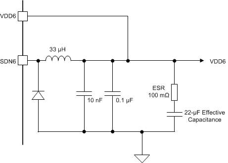 Figure 6-2 VDD6 Design
6.2.2.2 VDD1 Linear Controller
The microprocessor used with the TPS65381A-Q1 device requires a core voltage of 1.23 V.
The output voltage of the VDD1 linear controller is set by a resistor divider from the VDD1 output to ground with the divided voltage connected to the VDD1_SENSE pin, which must be set to 800 mV. To ensure sufficient bias current through the resistor divider, select a value of R1 as 80.6 Ω. Use Equation 2 to calculate the resistance of R2.
Select the standard value of 43.2 Ω.
NOTE
The tolerance of the R1 and R2 resistors in this resistor divider will impact the VDD1 regulation and voltage monitoring tolerance. Resistors with 0.1% tolerance are recommended.
Select an output FET for the VDD1 linear controller that meets the requirements in the VDD1 – LDO With External FET specifications in Section 4.5. An example output FET is BUK9213-30A. The gate of the output FET is connected to the VDD1_G pin. A 100-kΩ resistor is connected between the gate and source of the FET. The drain of the FET is connected to the VDD6 preregulator output, which is used as the supply input for the VDD1 linear controller.
A low-ESR ceramic output capacitor with 22-μF effective capacitance at 1.23 V is used to meet the requirements for the output capacitor that is listed in this data sheet. Depending on the application, this output may require a larger output capacitor to ensure the output does not drop below the required regulation specification during load transients. The VDD1 output capacitance is specified up to 40 μF.
Figure 6-3 shows this configuration.
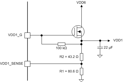 Figure 6-3 VDD1 Design
6.2.2.3 VSOUT1 Tracking Linear Regulator, Configured to Track VDD5
The system has a sensor that requires a 5-V supply that must track the VDD5 supply. The configuration should be set up for higher efficiency.
The VDD5 output is connected to the VTRACK1 pin, which configures the regulator for tracking mode. Because the output must track the input, unity gain feedback is used on the VSFB1 pin by connecting it to the VSOUT1 pin.
For efficiency, use the VDD6 preregulator as the supply. Therefore, the VDD6 output is connected to VSIN. A local, low-ESR 100-nF ceramic capacitor is used on the VSIN pin to stabilize the input.
A local, low-ESR 4.7-μF ceramic capacitor is used on the VSOUT1 output for loop stabilization. Depending on the application, this output may require a larger output capacitor to ensure that the output does not drop below the required regulation specification during load transients. The VSOUT1 output capacitance is specified up to 10 μF.
Figure 6-4 shows this configuration.
6.2.2.4 Alternative Use for VSOUT1 Tracking Linear Regulator, Configured for 6-V Output Tracking VDD3/5 In 3.3-V Mode
The system has a sensor that requires a 6-V supply that must track the VDD3/5 supply operating at 3.3 V.
The VDD3/5 supply, operating in 3.3-V mode, is connected to the VTRACK1 pin, which configures the regulator for tracking mode. Because the output must have gain to make the 6-V output track a 3.3-V supply, gain feedback is used on the VSFB1 pin. To achieve the required gain, connect a resistor divider the VSOUT1 and VSFB1 pins. Select a value of 3.3 kΩ for the RVSFB1 resistor to balance the current through the resistor divider for reasonable bias current and reasonable losses. Use Equation 3 to calculate the resistance of RVSFB2.
Select the standard value of 2.7 kΩ.
NOTE
The tolerance of the RVSFB1 and RVSFB2 resistors in this resistor divider will impact the VSOUT1 regulation and voltage monitoring tolerance. Resistors with 0.1% tolerance are recommended.
Because the desired VSOUT1 output is greater than 5 V, the VBATP supply must be used for the tracking supply. Therefore, connect the VBATP supply to the VSIN pin. A local, low-ESR 100-nF ceramic capacitor is used on the VSIN pin to stabilize the input.
A local, low-ESR 4.7-μF ceramic capacitor is used on the VSOUT1 pin for loop stabilization. Depending on the application, this output may require a larger output capacitor to ensure that the output does not drop below the required regulation specification during load transients. The VSOUT1 output capacitance is specified up to 10 μF.
Figure 6-5 shows this configuration.
6.2.2.5 Alternative Use for VSOUT1 Tracking Linear Regulator, Configured for 9-V Output Tracking to 5-V Input from VDD5
The system has a sensor that requires a 9-V supply that must track the VDD5 supply operating at 5 V.
The VDD5 supply is connected to VTRACK1, which configures the regulator for tracking mode. Because the output must have gain to make the 9-V output track a 5-V supply, gain feedback is used on the VSFB1 pin. To achieve the required gain, connect a resistor divider between the VSOUT1 and VSFB1 pins. Select a value of 3.3 kΩ for the RVSFB1 resistor to balance the current through the resistor divider for reasonable bias current and reasonable losses. Use Equation 4 to calculate the resistance of RVSFB2.
Select the standard value of 2.7 kΩ.
NOTE
The tolerance of the RVSFB1 and RVSFB2 resistors in this resistor divider will impact the VSOUT1 regulation and voltage monitoring tolerance. Resistors with 0.1% tolerance are recommended.
Because the desired VSOUT1 output is greater than 5-V, the VBATP supply must be used as the tracking supply. Therefore, connect the VBATP supply to the VSIN pin. A local, low-ESR 100-nF ceramic capacitor is used on the VSIN pin to stabilize the input.
A local, low-ESR 4.7-μF ceramic capacitor is used on the VSOUT1 pin for loop stabilization. Depending on the application, this output may require a larger output capacitor to ensure that the output does not drop below the required regulation specification during load transients. The VSOUT1 output capacitance is specified up to 10 μF.
Figure 6-6 shows this configuration.
6.2.2.6 Alternative Use for VSOUT1 Tracking Linear Regulator, Configured in Non-tracking Mode Providing a 4.5-V Output
If the system requires a 4.5-V supply that does not track any other supply, the VTRACK1 pin is connected to ground (GND), which configures the regulator for non-tracking mode. The output is now proportional to a fixed reference voltage (Vref) of 2.5 V on the VSFB1 pin. Because the output must have gain to result in a 4.5-V output, gain feedback will be used on the VSFB1 pin. To achieve the required gain, connect a resistor divider between the VSOUT1 and VSFB1 pins. Select a value of 3.3 kΩ for the RVSFB1 resistor to balance the current through the resistor divider for reasonable bias current and reasonable losses. Use Equation 5 to calculate the resistance of RVSFB2.
Select the standard value of 2.7 kΩ.
NOTE
The tolerance of the RVSFB1 and RVSFB2 resistors in this resistor divider will impact the VSOUT1 regulation and voltage monitoring tolerance. Resistors with 0.1% tolerance are recommended.
For efficiency, the VDD6 preregulator is the supply and therefore the VDD6 output is connected to the VSIN pin. A local, low-ESR 100-nF ceramic capacitor is used on the VSIN pin to stabilize the input.
A local, low-ESR 4.7-μF ceramic capacitor is used on the VSOUT1 pin for loop stabilization. Depending on the application, this output may require a larger output capacitor to ensure that the output does not drop below the required regulation specification during load transients. The VSOUT1 output capacitance is specified up to 10 μF.
Figure 6-7 shows this configuration.
6.2.3 Application Curves
For the application curves, see the figures listed in Table 6-1.
Table 6-1 Table of Graphs
| FIGURE TITLE | FIGURE NUMBER |
|---|---|
| SPI SDO Buffer Source and Sink Current | Figure 4-3 |
| VDD6 BUCK Efficiency | Figure 4-4 |
6.3 System Examples
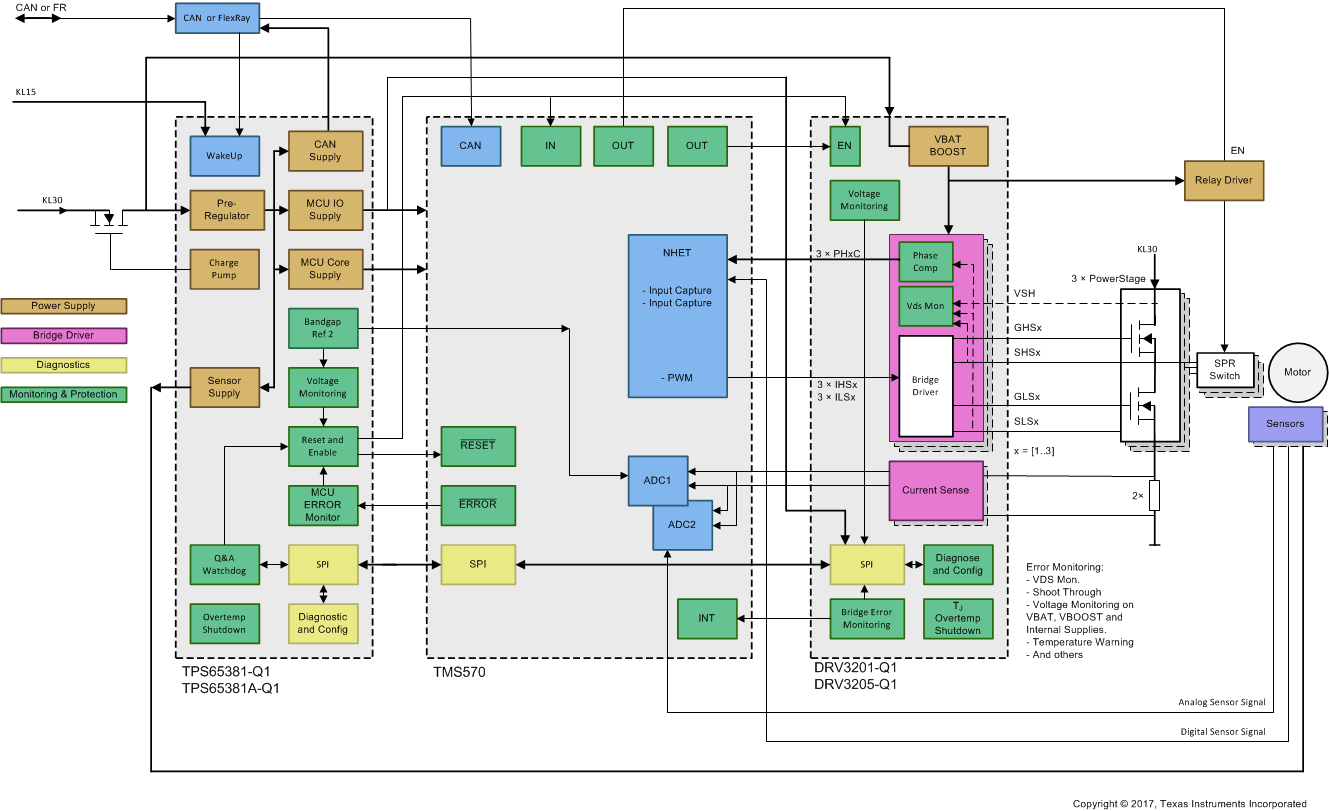 Figure 6-8 Electrical Power-Steering Example
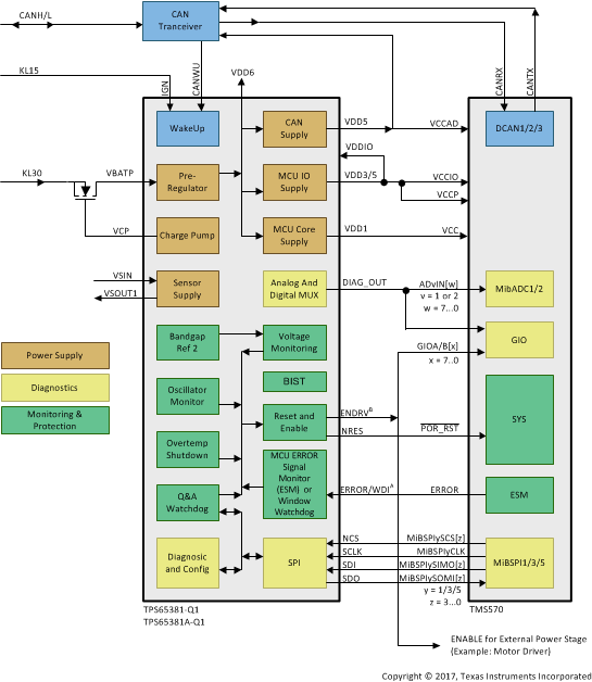
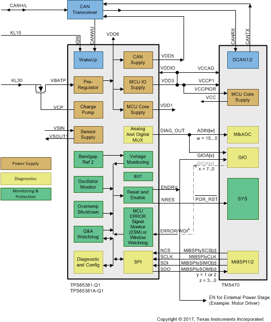
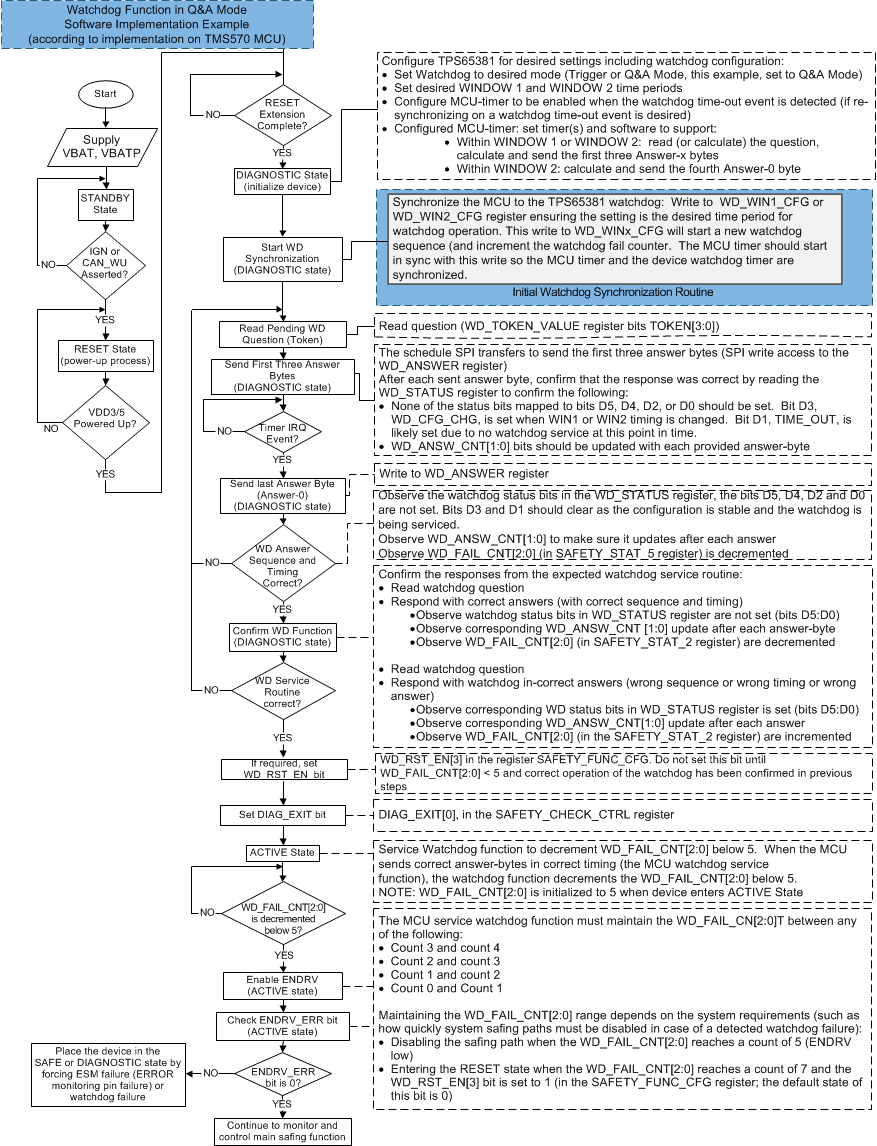 Figure 6-11 Software Flowchart for Configuring and Synchronizing the MCU With the Watchdog in Q&A Mode
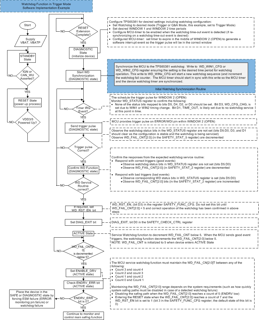 Figure 6-12 Software Flowchart for Configuring and Synchronizing the MCU With the Watchdog in Trigger Mode