SLVSBO3A December 2013 – December 2015 TPS657120
PRODUCTION DATA.
- 1 Device Overview
- 2 Revision History
- 3 Terminal Configuration and Functions
-
4 Specifications
- 4.1 Absolute Maximum Ratings
- 4.2 ESD Ratings
- 4.3 Recommended Operating Conditions
- 4.4 Thermal Information
- 4.5 Electrical Characteristics: General Functions
- 4.6 Electrical Characteristics: DCDC1 and DCDC2
- 4.7 Electrical Characteristics: DCDC3
- 4.8 Electrical Characteristics: RF-LDOs
- 4.9 Electrical Characteristics: Digital Inputs, Digital Outputs
- 4.10 Electrical Characteristics: Thermal Shutdown, Undervoltage Lockout
- 4.11 Electrical Characteristics: RFFE Timing Parameters
- 4.12 Typical Characteristics
-
5 Detailed Description
- 5.1 Overview
- 5.2 Functional Block Diagram
- 5.3
Feature Description
- 5.3.1 Default Settings
- 5.3.2 Linear Regulators
- 5.3.3 Step-down Converters DCDC1 and DCDC2
- 5.3.4 Power Save Mode
- 5.3.5 Dynamic Voltage Positioning (Optional)
- 5.3.6 Soft Start / Enable
- 5.3.7 Dynamic Voltage Scaling (DVS) for DCDC1, DCDC2 and DCDC3
- 5.3.8 100% Duty Cycle Low Dropout Operation
- 5.3.9 180° Out-of-Phase Operation
- 5.3.10 Undervoltage Lockout for DCDC1, DCDC2, DCDC3, LDO1 and LDO2
- 5.3.11 Output Voltage Discharge
- 5.3.12 Short-Circuit Protection
- 5.3.13 Output Voltage Monitoring
- 5.3.14 Step-Down Converter and LDO Enable; pins CLK_REQ1 and CLK_REQ2
- 5.3.15 Step-Down Converter DCDC3
- 5.3.16 DCDC3_SEL Control
- 5.3.17 Bypass Switch
- 5.3.18 DCDC3 Output Voltage Ramp Support
- 5.3.19 VCON Decoder
- 5.3.20 Thermal Monitoring and Shutdown
- 5.3.21 GPIOs
- 5.3.22 nRESET Input ; ADR_SELECT Input
- 5.3.23 Power State Machine
- 5.3.24 Implementation of Internal Power-Up and Power-Down Sequencing
- 5.3.25 VDDIO Voltage for Push-pull Output Stages / Interface
- 5.3.26 TPS657120 On Off Operation
- 5.3.27 MIPI RFFE Interface
- 5.4 Device Functional Modes
- 5.5 Register Maps
- 6 Application and Implementation
- 7 Power Supply Recommendations
- 8 Layout
- 9 Device and Documentation Support
- 10Mechanical, Packaging, and Orderable Information
8 Layout
8.1 Layout Guidelines
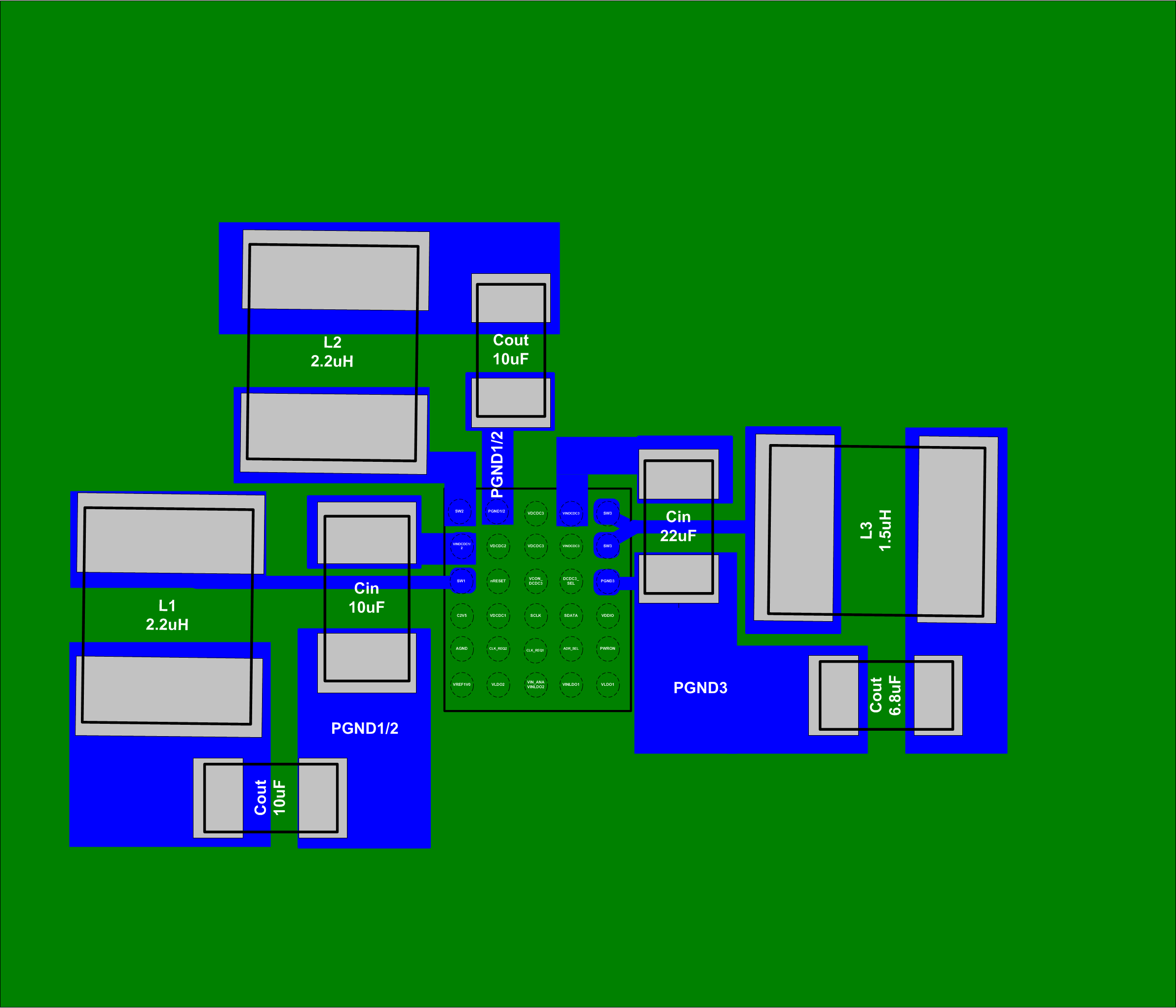
As for all switching power supplies, the layout is an important step in the design. Proper function of the device demands careful attention to PCB layout. Care must be taken in board layout to get the specified performance. If the layout is not carefully done, the regulators may show poor line and/or load regulation and stability issues as well as EMI problems. It is critical to provide a low impedance ground path. Therefore, use wide and short traces for the main current paths. The input capacitors must be placed as close as possible to the IC pins as well as the inductor and output capacitor.
Keep the common path to the GND pins, which returns the small signal components, and the high current of the output capacitors as short as possible to avoid ground noise. The VDCDCx trace should be connected right to the output capacitor and routed away from noisy components and traces (for example, the L1, L2, and L3 traces). See the EVM users guide for details about the layout for TPS657120.
