SLVSBO3A December 2013 – December 2015 TPS657120
PRODUCTION DATA.
- 1 Device Overview
- 2 Revision History
- 3 Terminal Configuration and Functions
-
4 Specifications
- 4.1 Absolute Maximum Ratings
- 4.2 ESD Ratings
- 4.3 Recommended Operating Conditions
- 4.4 Thermal Information
- 4.5 Electrical Characteristics: General Functions
- 4.6 Electrical Characteristics: DCDC1 and DCDC2
- 4.7 Electrical Characteristics: DCDC3
- 4.8 Electrical Characteristics: RF-LDOs
- 4.9 Electrical Characteristics: Digital Inputs, Digital Outputs
- 4.10 Electrical Characteristics: Thermal Shutdown, Undervoltage Lockout
- 4.11 Electrical Characteristics: RFFE Timing Parameters
- 4.12 Typical Characteristics
-
5 Detailed Description
- 5.1 Overview
- 5.2 Functional Block Diagram
- 5.3
Feature Description
- 5.3.1 Default Settings
- 5.3.2 Linear Regulators
- 5.3.3 Step-down Converters DCDC1 and DCDC2
- 5.3.4 Power Save Mode
- 5.3.5 Dynamic Voltage Positioning (Optional)
- 5.3.6 Soft Start / Enable
- 5.3.7 Dynamic Voltage Scaling (DVS) for DCDC1, DCDC2 and DCDC3
- 5.3.8 100% Duty Cycle Low Dropout Operation
- 5.3.9 180° Out-of-Phase Operation
- 5.3.10 Undervoltage Lockout for DCDC1, DCDC2, DCDC3, LDO1 and LDO2
- 5.3.11 Output Voltage Discharge
- 5.3.12 Short-Circuit Protection
- 5.3.13 Output Voltage Monitoring
- 5.3.14 Step-Down Converter and LDO Enable; pins CLK_REQ1 and CLK_REQ2
- 5.3.15 Step-Down Converter DCDC3
- 5.3.16 DCDC3_SEL Control
- 5.3.17 Bypass Switch
- 5.3.18 DCDC3 Output Voltage Ramp Support
- 5.3.19 VCON Decoder
- 5.3.20 Thermal Monitoring and Shutdown
- 5.3.21 GPIOs
- 5.3.22 nRESET Input ; ADR_SELECT Input
- 5.3.23 Power State Machine
- 5.3.24 Implementation of Internal Power-Up and Power-Down Sequencing
- 5.3.25 VDDIO Voltage for Push-pull Output Stages / Interface
- 5.3.26 TPS657120 On Off Operation
- 5.3.27 MIPI RFFE Interface
- 5.4 Device Functional Modes
- 5.5 Register Maps
- 6 Application and Implementation
- 7 Power Supply Recommendations
- 8 Layout
- 9 Device and Documentation Support
- 10Mechanical, Packaging, and Orderable Information
4 Specifications
4.1 Absolute Maximum Ratings
over operating free-air temperature range (unless otherwise noted)(1)| MIN | MAX | UNIT | |||
|---|---|---|---|---|---|
| Voltage | all pins except A/PGND pins and pins listed below with respect to AGND | –0.3 | 6 | V | |
| VLDO1, VLDO2, VDDIO with respect to AGND | –0.3 | 3.6 | V | ||
| pin VDCDC3 with respect to AGND | –0.3 | 5.5 | V | ||
| pins SDATA, SCLK, DCDC3_SEL , GPIO_0, GPIO_1, CLK_REQ1, CLK_REQ2 , with respect to AGND | –0.3 | VDDIO + 0.3 | V | ||
| Current | all non power pins | 5 | mA | ||
| power pins | 2 | A | |||
| TA | Operating free-air temperature | –40 | 85 | °C | |
| TJ | Maximum junction temperature | 125 | °C | ||
| Tstg | Storage temperature | –65 | 150 | °C | |
(1) Stresses beyond those listed under Absolute Maximum Ratings may cause permanent damage to the device. These are stress ratings only and functional operation of the device at these or any other conditions beyond those indicated under Section 4.3 is not implied. Exposure to absolute-maximum-rated conditions for extended periods may affect device reliability.
4.2 ESD Ratings
| VALUE | UNIT | |||
|---|---|---|---|---|
| V(ESD) | Electrostatic discharge | Human body model (HBM), per ANSI/ESDA/JEDEC JS-001, all pins(1) | 2000 | V |
| Charged device model (CDM), per JEDEC specification JESD22-C101, all pins(2) | 500 | |||
(1) JEDEC document JEP155 states that 500-V HBM allows safe manufacturing with a standard ESD control process.
(2) JEDEC document JEP157 states that 250-V CDM allows safe manufacturing with a standard ESD control process.
4.3 Recommended Operating Conditions
over operating free-air temperature range (unless otherwise noted)| MIN | NOM | MAX | UNIT | |||
|---|---|---|---|---|---|---|
| DCDC CONVERTERS | ||||||
| VINDCDC1, VINDCDC2, VINDCDC3 |
Input voltage range for step-down converter DCDC1, DCDC2, DCDC3 | 2.8 | 5.5 | V | ||
| Output voltage range for step-down converter | DCDC1, DCDC2 | 0.8 | 3.3 | V | ||
| DCDC3 | 0.1 | 3.6 | V | |||
| L1, L2 | Inductance at L1, L2 | 1 | 2.2 | 2.9 | μH | |
| L3 | Inductance at L3 | 1 | 1.5 | 2.2 | μH | |
| CVINDCDC1/2 | Input capacitance at VINDCDC1/2 (1) | 4.7 | 10 | μF | ||
| CVINDCDC3 | Input capacitance at VINDCDC3 (1) | 10 | 22 | μF | ||
| COUTDCDC1,2 | Output capacitance at DCDC1 and DCDC2 (1) | 4.7 | 10 | 22 | μF | |
| COUTDCDC3 | Output capacitance at DCDC3 (1) | 2.0 | 6 | 12 | μF | |
| LDOs; GENERIC | ||||||
| VINLDO1 | Input voltage range for LDO1 | 2.0 | 5.5 | V | ||
| VINLDO2(2) | Input voltage for LDO2(3) | 2.8 | 5.5 | V | ||
| VLDO1, VLDO2 | Output voltage for LDOs | 1.2 | 3.4 | V | ||
| CINLDO1
CINLDO2 |
Input capacitance on LDO supply pins (1) | 0.5 | μF | |||
| CoutLDO1,
CoutLDO2 |
Output capacitance on LDO1, LDO2 (1) | 1 | 4.7 | μF | ||
| VVDDIO | for RFFE interface at 1.2 V or 1.8 V | 1.1 | 1.95 | V | ||
| CVDDIO | Input capacitance on VDDIO | 100 | nF | |||
| C(C2V5) | Capacitance at internal supply at pin C2V5 | 0.5 | 1 | 10 | μF | |
| C(VREF1V0) | Bypass capacitance at internal reference VREF1V0 | 47 | 100 | 220 | nF | |
| TA | Operating ambient temperature | –40 | 85 | °C | ||
| TJ | Operating junction temperature | –40 | 125 | °C | ||
(1) Ceramic capacitors show an effect called DC Bias Effect. With a dc voltage applied to a ceramic capacitor , the effective capacitance is reduced. The table above therefore lists the minimum value as Capacitance. In order to meet the minimum capacitance, the nominal value may have to be scaled accordingly to take the drop of capacitance into account for a given dc voltage at the LDOs of dcdc converters. Input capacitors need to be placed as close as possible to the pins of TPS657120.
(2) Analog supply voltage VIN_ANA
(3) As this pin is used as the analog supply voltage, it needs to be tied to VINDCDCx
4.4 Thermal Information
| THERMAL METRIC(1) | TPS657120 | UNIT | |
|---|---|---|---|
| YFF (DSBGA) | |||
| 30 PINS | |||
| RθJA | Junction-to-ambient thermal resistance | 58.8 | °C/W |
| RθJC(top) | Junction-to-case (top) thermal resistance | 0.3 | °C/W |
| RθJB | Junction-to-board thermal resistance | 27.0 | °C/W |
| ψJT | Junction-to-top characterization parameter | 1.4 | °C/W |
| ψJB | Junction-to-board characterization parameter | 26.9 | °C/W |
(1) For more information about traditional and new thermal metrics, see the Semiconductor and IC Package Thermal Metrics application report (SPRA953).
4.5 Electrical Characteristics: General Functions
TA = –40°C to +85°C, typical values are at TA = 25°C (unless otherwise noted), see Section 4.12.| PARAMETER | TEST CONDITIONS | MIN | TYP | MAX | UNIT | |
|---|---|---|---|---|---|---|
| ISB | Standby supply current | PWRON=LOW; total current in STANDBY state into pins VINDCDC1/2, VINDCDC3 and VIN_ANA | 55 | μA | ||
| IQ | Quiescent supply current | PWRON=HIGH, LDOs and DCDC converters =OFF | 60 | μA | ||
| IQ | Quiescent supply current | PWRON=HIGH, LDO1 and LDO2 and DCDC1 and DCDC2 = enabled in normal mode | 170 | μA | ||
4.6 Electrical Characteristics: DCDC1 and DCDC2
TA = –40°C to +85°C, typical values are at TA = 25°C (unless otherwise noted); see Section 4.12.| PARAMETER | TEST CONDITIONS | MIN | TYP | MAX | UNIT | |
|---|---|---|---|---|---|---|
| VIN | Input voltage | 2.8 | 5.5 | V | ||
| VDCDC1
VDCDC2 |
DCDCx output voltage | 25-mV steps up to 2.2 V; 50-mV steps above 2.2 V | 0.8 | 3.3 | V | |
| VDCDC1
VDCDC2 |
Default output voltage | VDCDC1 | 1.7 | V | ||
| VDCDC2 | 2.65 | |||||
| IOUT(DCDCx) | Continuous output current | DCDC1 (VINDCDC1 ≥ 2.8 V) | 300 | mA | ||
| DCDC2 (VINDCDC2 ≥ 2.8 V) | 250 | |||||
| IQ | Quiescent current | ILOAD = 0 mA, DCDCx_MODE = 0, Device not switching; for each DCDC1 and DCDC2 | 16 | 25 | μA | |
| ILOAD = 0 mA, DCDCx_MODE = 1, Device switching; for each DCDC1 and DCDC2 | 3.5 | mA | ||||
| VDCDC1/2 | Accuracy | DCDCx_MODE = 1, VIN = 3.0 V to 5.5 V, ILOAD = 0 mA, tolerance is ±2% or ±25 mV whatever is larger | –2% | 2% | ||
| DCDCx_MODE = 0, VIN = 3.0 V to 5.5 V, ILOAD = 0 mA, +1% voltage scaling active | –3% | 1.25% | 3.5% | |||
| Load regulation | DCDCx_MODE = 1, VIN = 3.0 V to 5.5 V; ILOAD = 25 mA to 225 mA; for DCDC1 and DCDC2 | 0.25 | %/A | |||
| fSW | Switching frequency | DCDCx_MODE = 1, VIN = 3.0 V to 5.5 V | 1.9 | 2.4 | 2.6 | MHz |
| RDS(ON) | High-side FET On-resistance | For DCDC1 and DCDC2 with VINDCDCx = 3.6 V, D = 100% | 250 | 400 | mΩ | |
| RDS(ON) | Low-side FET On-resistance | For DCDC1 and DCDC2 with VINDCDCx = 3.6 V, D = 100% | 220 | 350 | mΩ | |
| ILK_HS | High-side FET leakage current | TJ = 85°C; DCDC1, DCDC2; VINDCDC1 = VINDCDC2 = 5.5 V | 2 | μA | ||
| ILK_LS | Low-side FET leakage current | TJ = 85°C; DCDC1, DCDC2; VINDCDC1 = VINDCDC2 = 5.5 V | 3 | μA | ||
| IHS_LIMF | High-side forward current limit | 2.9 V ≤ VIN_DCDC1 ≤ 5.5 V; for DCDC1 | 500 | 650 | 800 | mA |
| ILS_LIMF | Low-side forward current limit | 2.9 V ≤ VIN_DCDC1 ≤ 5.5 V; for DCDC1 | 500 | 650 | 800 | mA |
| IHS_LIMF | High-side forward current limit | 2.9 V ≤ VIN_DCDC2 ≤ 5.5 V; for DCDC2 | 425 | 600 | 775 | mA |
| ILS_LIMF | Low-side forward current limit | 2.9 V ≤ VIN_DCDC2 ≤ 5.5 V; for DCDC2 | 425 | 600 | 775 | mA |
| DCDC1, DCDC2 output voltage ripple | VIN = 3.6 V; VOUT = 1.7 V to 2.65 V; Io = 10 mA to 300 mA; L = 1.5uH, RSL = 50 mR; Co = 10 µF | 10 | 25 | mVpp | ||
| Efficiency | VINDCDCx = 3.7 V, Vo = 1.7 V or Vo = 2.65 V; Io = 80 mA to 150 mA | 88% | 93% | |||
| VINDCDCx = 3.7 V, Vo = 1.7 V or Vo = 2.65 V; Io = 300 µA | 80% | |||||
| VINDCDCx = 3.7 V, Vo = 1.7 V or Vo = 2.65 V; Io = 100 µA | 45% | |||||
| Pulse skipping threshold | Output current when device switches from PFM to PWM automatically; VIN = 3.6 V, VOUT = 1.7 V | 140 | mA | |||
| output current when device switches from PFM to PWM automatically; VIN = 3.6 V, VOUT = 2.65 V | 60 | |||||
| PSRR | Power supply rejection ratio | VIN = 3.6 V, ILOAD = 150 mA, 10 Hz < f < 10 kHz, Vo = 1.7 V and Vo = 2.65 V | 40 | dB | ||
| Output noise | VIN = 3.6 V, ILOAD = 100 mA, Vo = 1.7 V and Vo = 2.65 V | μV/√Hz | ||||
| 1 kHz < f < 100 kHz | 2 | |||||
| 100 kHz < f < 1 MHz | 0.2 | |||||
| 1 MHz < f < 10 MHz; not including f(sw) | 0.1 | |||||
| VDCDCPG-falling | Power good threshold | VDCDCx falling | VDCDCx –15% | VDCDCx – 7% | ||
| VDCDCPG-rising | Power good threshold | VDCDCx rising | VDCDCx – 3% | |||
| tStart | Start-up time | Time to start switching, measured from end of MIPI command enabling converter | 225 | μs | ||
| tRamp | VOUT Ramp UP time | Time to ramp from 5% to 95% of VOUT | 200 | μs | ||
| RDischarge | Discharge resistor | 250 | 400 | 600 | Ω | |
4.7 Electrical Characteristics: DCDC3
TA = –40°C to +85°C, typical values are at TA = 25°C (unless otherwise noted); see Section 4.12.| PARAMETER | TEST CONDITIONS | MIN | TYP | MAX | UNIT | |
|---|---|---|---|---|---|---|
| VIN | Input voltage | 2.8 | 5.5 | V | ||
| VDCDC3 | DCDC3 output voltage | output voltage defined by internal resistor divider; DCDC3_CTRL:VCON = 0 | 0.8 | 3.60 | V | |
| output voltage defined by VCON input; DCDC3_CTRL:VCON = 1 | 0.1 | 3.60 | ||||
| IOUT(DCDC3) | Continuous output current | DCDC3 | 2200 | mA | ||
| IQ | Quiescent current | ILOAD = 0 mA, DCDC3_MODE = 0, Device not switching | 26 | 46 | μA | |
| ILOAD = 0 mA, DCDC3_MODE = 1, Device switching | 6 | mA | ||||
| VDCDC3 | Accuracy; output voltage setting with register; DCDC3_CTRL:VCON = 0 | DCDC3_MODE = 1, ILOAD = 0 mA, TA = 25°C; COUT = 2 x 4.7 µF + 2.2 µF |
–2% | 2% | ||
| DCDC3_MODE = 1, ILOAD = 0 mA, TA = –40 – 85°C; COUT = 2 x 4.7 µF + 2.2 µF |
–2.5% | 2.5% | ||||
| DCDC3_MODE = 0, ILOAD = 0 mA, TA = 25°C; COUT = 2 x 4.7 µF + 2.2 µF the output voltage tolerance is ±3% or ±45 mV whichever is larger |
–3% | 3% | ||||
| DCDC3_MODE = 0, ILOAD = 0 mA, TA = –40 – 85°C; COUT = 2 x 4.7 µF + 2.2 µF the output voltage tolerance is ±3% or ±45 mV whichever is larger |
–3% | 3% | ||||
| Accuracy for VCON operation; DCDC3_CTRL:VCON = 1 | Vo = 0.1 V to 3.6 V; COUT = 2 x 4.7 µF + 2.2 µF; PWM mode forced automatically; accuracy in VCON mode is ±5% or ±25 mV, whichever is larger |
–5% | 5% | |||
| fSW | Switching frequency | DCDC3_MODE = 1 or DCDC3_CTRL:VCON = 1 | 2100 | 2300 | 2700 | kHz |
| RDS(ON) | High-side MOSFET on-resistance | VIN_DCDC3 = 3.6 V, 100% duty cycle | 75 | 120 | mΩ | |
| Low-side MOSFET on-resistance | VIN_DCDC3 = 3.6 V, 0% duty cycle | 110 | 180 | mΩ | ||
| ILK_HS | High-side leakage current | TJ = 85°C; VINDCDC3=4.2 V | 3 | μA | ||
| ILK_LS | Low-side leakage current | TJ = 85°C; VINDCDC3=4.2 V | 3 | μA | ||
| ILIM | High-side current limit | 2.9 V ≤ VIN_DCDC3 ≤ 5.5 V | 2400 | 3000 | 3600 | mA |
| ILIM | Low-side current limit | 2.9 V ≤ VIN_DCDC3 ≤ 5.5 V | 2200 | 2800 | 3400 | mA |
| ILIM | Low-side negative current limit | 2.9 V ≤ VIN_DCDC3 ≤ 5.5 V; EN_nILIM_xl=1 | 1000 | 1500 | 2000 | mA |
| 2.9 V ≤ VIN_DCDC3 ≤ 5.5 V; EN_nILIM_xl=0 | 200 | mA | ||||
| Duty cycle | VIN = 3.6 V | 2% | 100% | |||
| DCDC3 output voltage ripple | VIN = 5 V; VOUT = 3.4 V; Io=2 A; L=1.5 µH, ESR=90 mR; Co=10 µF | 10 | 50 | mVpp | ||
| DCDC3 load transient response | VIN = 5 V; VOUT = 3.4 V; Io=200 mA to 1.8 A; L=1.5 µH, ESR=90 mR; Co=10 µF; dt=10 µs | 100 | mV | |||
| Efficiency | VINDCDCx=3.7 V, Vo=3.4 V; Io=1500 mA | 80% | ||||
| VINDCDCx=3.7 V, Vo=3.4 V; Io=400 mA | 90% | |||||
| VINDCDCx=3.7 V, Vo=2.0 V; Io=10 mA | 80% | |||||
| Output noise | VIN = 3.6 V, ILOAD = 100 mA, Vo=2.65 V | μV/√Hz | ||||
| 1 kHz < f < 100 kHz | 3 | |||||
| 100 kHz < f < 1 MHz | 0.2 | |||||
| 1 MHz < f < 10 MHz | 0.1 | |||||
| VDCDCPG-falling | Power good threshold | VDCDCx falling | VDCDCx - 14% | VDCDCx - 7% | ||
| VDCDCPG-rising | Power good threshold | VDCDCx rising | VDCDCx - 5% | |||
| tStart | Start-up time | Time to start switching, measured from end of RFFE command enabling converter | 175 | μs | ||
| tRamp | VOUT Ramp UP time | Time to ramp from 5% to 95% of VOUT ; DCDC3_CTRL:IMMEDIATE = 1; VOUT = 3.4 V | 30 | μs | ||
| Rise and fall time | dVo=±1 V; Io=450 mA; Co=10 µF; DCDC3_SEL mode | 30 | μs | |||
| Ramp time in VCON mode | 10 | μs | ||||
| VCON input voltage | 0.2 | 2.1 | V | |||
| VCON slew rate | 300 | mV/μs | ||||
| VCON input resistance | 1 | MΩ | ||||
| VCON gain | Typical adjustable range | 1.3 | 2.7 | |||
| VCON offset | –350 | 0 | mV | |||
| RDischarge | Discharge resistor | 250 | 400 | 500 | Ω | |
| Voltage between VINDCDC3 and VDCDC3 | 5.5 | V | ||||
| Bypass switch current limit | VINDCDCx= 2.8 V to 5.5 V; not tested in production | 2000 | 2500 | 3000 | mA | |
| Bypass switch current limit response time | 10 | µs | ||||
| Resistance from VINDCDC3 to VDCDC3 | Bypass switch closed; not including the parallel path through high side switch and inductor | 100 | 170 | mΩ | ||
| Leakage current from VINDCDC3 to VDCDC3 | When bypass switch is open | 10 | µA | |||
| Bypass switch over-voltage protection | Sensed at VDCDC3; bypass enabled bit is cleared when voltage is exceeded; rising edge | 4.0 | V | |||
| Sensed at VDCDC3; bypass enabled bit is cleared when voltage is exceeded; falling edge | 3.7 | |||||
4.8 Electrical Characteristics: RF-LDOs
TA = –40°C to +85°C, typical values are at TA = 25°C (unless otherwise noted); see Section 4.12.| PARAMETER | TEST CONDITIONS | MIN | TYP | MAX | UNIT | |
|---|---|---|---|---|---|---|
| VIN | Input voltage | LDO1 | 2.0 | 5.5 | V | |
| LDO2, analog supply voltage input | 2.8 | 5.5 | ||||
| VLDOx | LDO output voltage for RF-LDOs | 50-mV steps | 1.2 | 3.4 | V | |
| LDO voltage accuracy | ECO = 0 | –2% | 2% | |||
| ECO = 1 | –5% | 5% | ||||
| IOUT(LDOx) | LDO continuous output current | LDO1 | 10 | mA | ||
| LDO2 | 10 | |||||
| ISHORT(LDOx) | LDO current limit | LDO1 | 20 | 80 | mA | |
| LDO2 | 20 | 80 | ||||
| VDO(LDOx) | Dropout voltage (1) | IOUT(LDO1) = 10 mA; VINLDO1=2.0 V | 250 | mV | ||
| IOUT(LDO2) = 10 mA; VINLDO2=3.0 V | 250 | |||||
| Line regulation | VIN = VLDO + 0.5 V & ILOAD = 10 mA for LDO1 and for LDO2 | –1% | 1% | |||
| Load regulation; ECO = 0 | LDO1 and LDO2: ILOAD = 50 µA to 10 mA | 40 | mV | |||
| Load regulation; ECO = 1 | LDO1 and LDO2: ILOAD = 0 mA to 1 mA | –5% | 5% | |||
| Line transient response | dV/dt = ±0.5 V/μs | –50 | 50 | mV | ||
| Load transient response | for LDO1 and LDO2: dI/dt = 100 mA/μs; 1-mA to 10-mA load step | 50 | mV | |||
| PSRR | Power supply rejection ratio | f = 10 Hz to 1 kHz, VIN - VOUT ≥ 0.5 V, ILOAD = 10 mA | 63 | dB | ||
| Output voltage noise | f = 10 Hz to 100 kHz, VIN - VOUT ≥ 0.5 V , ILOAD = 10 mA | 30 | µVrms | |||
| Iq | Quiescent current | ECO = 1; ILOAD ≤ 1 mA for LDO1, LDO2 | 16 | µA | ||
| ECO = 0; ILOAD ≤ 10 mA for LDO1, LDO2 | 40 | µA | ||||
| ECO exit time | Minimum wait time before the full current can be drawn after ECO is set 0 | 50 | µs | |||
| tRamp | VOUT ramp up time | Time to ramp from 5% to 95% of VOUT ; IOUT = 10 mA; Co=4.7 µF; Vo=1.8 V |
850 | 1000 | µs | |
| tRamp | VOUT ramp up time | Time to ramp from 5% to 95% of VOUT ; IOUT = 10 mA; Co=4.7 µF; Vo=2.8 V |
1000 | 1200 | µs | |
| VLDOPG-falling | Power good threshold | VDCDCx falling | VLDOx - 14% | VLDOx - 7% | ||
| VLDOPG-rising | Power good threshold | VDCDCx rising | VLDOx - 5% | |||
| RDischarge | Discharge resistance at LDOx output | LDOx disabled | 200 | 325 | 450 | Ω |
(1) VDO = VIN - VOUT, where VOUT = VOUT(NOM) - 2%
4.9 Electrical Characteristics: Digital Inputs, Digital Outputs
TA = –40°C to +85°C, typical values are at TA = 25°C (unless otherwise noted)| PARAMETER | TEST CONDITIONS | MIN | TYP | MAX | UNIT | ||
|---|---|---|---|---|---|---|---|
| RFFE INTERFACE | |||||||
| VVDDIO | VDDIO voltage | VDDIO = 1.2 V | 1.1 | 1.2 | 1.3 | V | |
| VDDIO = 1.8 V | 1.65 | 1.8 | 1.95 | V | |||
| IVIO-IN | I/O voltage average input current for SDATA, SCLK | VDDIO=1.8 V; average during a 26-MHz write | 1.25 | mA | |||
| CL | Load capacitance | Half-speed readback; not including TPS657120 pin capacitance | 50 | pF | |||
| VOL | Low level output voltage for SDATA, SCLK | IOL= 2 mA | 0 | 0.2 × VDDIO | V | ||
| VOH | High level output voltage for SDATA, SCLK | IOH= –2 mA | 0.8 × VDDIO | VDDIO | V | ||
| VTP | INPUT: Positive going threshold voltage | VDDIO = 1.2 V or 1.8 V | 0.4 × VDDIO | 0.7 × VDDIO | V | ||
| VTN | INPUT: Negative going threshold voltage | VDDIO = 1.2 V | 0.28 × VDDIO | 0.6 × VDDIO | V | ||
| VTN | INPUT: Negative going threshold voltage | VDDIO = 1.8 V | 0.3 × VDDIO | 0.6 × VDDIO | V | ||
| VH | INPUT: Hysteresis voltage (VTP-VTN) | VDDIO = 1.2 V or 1.8 V | 0.1 × VDDIO | 0.4 × VDDIO | V | ||
| VIORST | RFFE I/O voltage reset voltage level | RFFE interface is in reset when VDDIO is below that voltage | 0.95 | V | |||
| IIH | SDATA = 0.8 x VDDIO | –2 | 10 | uA | |||
| SCLK = 0.8 x VDDIO | –1 | 10 | |||||
| IIL | SDATA = 0.2 x VDDIO | –2 | 5 | uA | |||
| SCLK = 0.2 x VDDIO | –1 | 1 | |||||
| GENERIC I/Os | |||||||
| VIL | Low-level input voltage | PWRON | 0 | 0.4 | V | ||
| GPIO_0, GPIO_1, CLK_REQ1, CLK_REQ2 , DCDC3_SEL; SDATA, SCLK | 0 | 0.3 × VDDIO | |||||
| VIH | High-level input voltage | PWRON | 1.1 | Vcc | V | ||
| GPIO_0, GPIO_1, CLK_REQ1, CLK_REQ2 , DCDC3_SEL, SDATA, SCLK | 0.7 × VDDIO | VDDIO | |||||
| VOL | Low-level output voltage | IOL= 1 mA for VDDIO=1.8 V | 0 | 0.2 | V | ||
| VOH | High-level output voltage | For pins configured as push-pull ouput to VDDIO; IOH= 1 mA for VDDIO=1.8 V | VDDIO - 0.2 | VDDIO | V | ||
| For pins configured as open-drain ouput | Vcc | ||||||
| IOL | Low-level output current Low-level output current | VDDIO ≥ 1.8 V | 1 | mA | |||
| VDDIO = 1.2 V | 0.1 | ||||||
| IOH | High-level output current | VDDIO ≥ 1.8 V | 1 | mA | |||
| VDDIO = 1.2 V | 0.1 | ||||||
| ILKG | Input leakage current | Input pins tied to VILor VIH | 0.2 | µA | |||
| TdHL | CLK_REQ1, CLK_REQ2, DCDC3_SEL delay for HIGH to LOW change | 2 | µs | ||||
| TdLH | CLK_REQ1, CLK_REQ2, DCDC3_SEL delay for LOW to HIGH change | 2 | µs | ||||
| TdLH | PWRON delay for LOW to HIGH change | For TPS657120 in STANDBY mode going to ACTIVE | 4 | 30% | ms | ||
4.10 Electrical Characteristics: Thermal Shutdown, Undervoltage Lockout
TA = –40°C to +85°C, typical values are at TA = 25°C (unless otherwise noted)| PARAMETER | TEST CONDITIONS | MIN | TYP | MAX | UNIT | |
|---|---|---|---|---|---|---|
| Thermal shutdown temperature rising threshold | 136 | 148 | 160 | °C | ||
| Thermal shutdown temperature hysteresis | Temperature falling | 20 | °C | |||
| UVLO threshold | Supply voltage rising | 2.7 | V | |||
| UVLO threshold | Supply voltage falling | 2.6 | V | |||
4.11 Electrical Characteristics: RFFE Timing Parameters
TA = –40°C to +85°C, typical values are at TA = 25°C (unless otherwise noted)| MIN | NOM | MAX | UNIT | |||
|---|---|---|---|---|---|---|
| fCLK | SCLK frequency | For write access | 0.032 | 26 | MHz | |
| fCLK_HALF | SCLK half-speed frequency | For read access | 0.032 | 13 | MHz | |
| TSCLKIH | SCLK input high time | For full-speed write access | 11.25 | ns | ||
| TSCLKIL | SCLK input low time | For full-speed write access | 11.25 | ns | ||
| TS | Data setup time | VDDIO = 1.8 V | 1 | ns | ||
| VDDIO = 1.2 V | 4 | |||||
| TH | Data hold time | 5 | ns | |||
| TD | Time for data output valid from SCLK rising edge | TPS657120 is a half-speed device for read operations | 0 | 22 | ns | |
| TSDATAOTRL | SDATA output transition (rise/fall) time | 2.1 | 6.5 | ns | ||
| TSDATAZ | Data drive release time | 10 | ns | |||
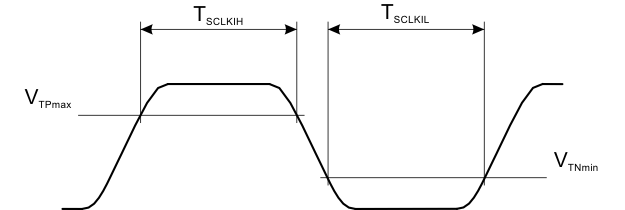 Figure 4-1 MIPI RFFE Received Clock Signal Constraints
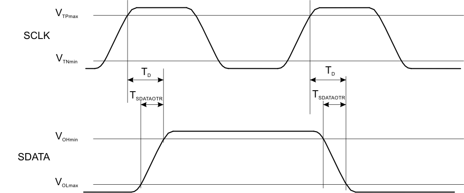 Figure 4-2 MIPI RFFE Bus Active Data Transmission Timing Specification
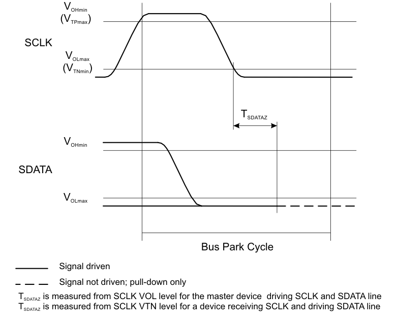 Figure 4-3 MIPI RFFE Bus Park Cycle Timing
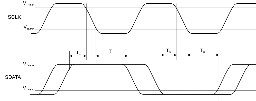 Figure 4-4 MIPI RFFE Data Setup and Hold Timing
4.12 Typical Characteristics
at TA = 25°C (unless otherwise noted)The graphs have been generated using the evaluation module (EVM) with the passive components as specified in the recommended operating conditions unless listed below at TA = 25°C, unless otherwise specified:
- L1 = L2 = DFE201610C-2R2
- L3 = DFE252010-1R5
- CoutDCDC1,2 = 10 µF (GRM188R61A106ME69)
- CoutDCDC3 = 4.7 µF + 2.2 µF (GRM188R60J475KE19 + GRM185R60J225)
- CoutLDO1,2 = 4.7 µF (GRM188R60J475KE19)
Table 4-1 Table of Graphs
| FIGURE | |||
|---|---|---|---|
| Efficiency DCDC1 vs Load current / PWM mode | VO = 1.7 V; VI = 3.0 V, 3.8 V, 4.2 V, 5.0 V | Figure 4-5 | |
| Efficiency DCDC1 vs Load current / PFM mode | VO = 1.7 V; VI = 3.0 V, 3.8 V, 4.2 V, 5.0 V | Figure 4-6 | |
| Efficiency DCDC2 vs Load current / PWM mode | VO = 2.65 V; VI = 3.0 V, 3.8 V, 4.2 V, 5.0 V | Figure 4-7 | |
| Efficiency DCDC2 vs Load current / PFM mode | VO = 2.65 V; VI = 3.0 V, 3.8 V, 4.2 V, 5.0 V | Figure 4-8 | |
| Efficiency DCDC3 vs Load current / PWM mode | VO = 0.85 V; VI = 3.0 V, 3.8 V, 4.2 V, 5.0 V | Figure 4-9 | |
| Efficiency DCDC3 vs Load current / PFM mode | VO = 0.85 V; VI = 3.0 V, 3.8 V, 4.2 V, 5.0 V | Figure 4-10 | |
| Efficiency DCDC3 vs Load current / PWM mode | VO = 2.0 V; VI = 3.0 V, 3.8 V, 4.2 V, 5.0 V | Figure 4-11 | |
| Efficiency DCDC3 vs Load current / PFM mode | VO = 2.0 V; VI = 3.0 V, 3.8 V, 4.2 V, 5.0 V | Figure 4-12 | |
| Efficiency DCDC3 vs Load current / PWM mode | VO = 3.4 V; VI = 3.6 V, 3.8 V, 4.2 V, 5.0 V | Figure 4-13 | |
| Efficiency DCDC3 vs Load current / PFM mode | VO = 3.4 V; VI = 3.6 V, 3.8 V, 4.2 V, 5.0 V | Figure 4-14 | |
| Load transient response DCDC1 in PWM mode | IO= 30 mA to 270 mA; VO = 1.7 V; VI = 3.6 V | Figure 4-15 | |
| Load transient response DCDC1 in PFM mode | IO= 30 mA to 270 mA; VO = 1.7 V; VI = 3.6 V | Figure 4-16 | |
| Load transient response DCDC2 in PWM mode | IO= 30 mA to 270 mA; VO = 2.65 V; VI = 3.6 V | Figure 4-17 | |
| Load transient response DCDC2 in PFM mode | IO= 30 mA to 270 mA; VO = 2.65 V; VI = 3.6 V | Figure 4-18 | |
| Load transient response DCDC3 in PFM mode | IO= 100 mA to 900 mA; VO = 2.0 V; VI = 3.6 V | Figure 4-19 | |
| Load transient response DCDC3 in PFM mode | IO= 200 mA to 1800 mA; VO = 3.4 V; VI = 3.8 V | Figure 4-20 | |
| Line transient response DCDC1 in PWM mode | VO= 1.7 V; VI = 3.6 V to 4.2 V; IO= 100 mA | Figure 4-21 | |
| Line transient response DCDC1 in PFM mode | VO= 1.7 V; VI = 3.6 V to 4.2 V; IO= 100 mA | Figure 4-22 | |
| Line transient response DCDC2 in PWM mode | VO= 2.65 V; VI = 3.6 V to 4.2 V; Load = 26.5 Ω at 100 mA | Figure 4-23 | |
| Line transient response DCDC2 in PFM mode | VO= 2.65 V; VI = 3.6 V to 4.2 V; Load = 26.5 Ω at 100 mA | Figure 4-24 | |
| Line transient response DCDC3 in PFM mode | VO = 2.0 V; VI= 3.6 V to 4.2 V; Load = 1.6 Ω at 1.25 A | Figure 4-25 | |
| Line transient response DCDC3 in PFM mode | VO = 3.4 V; VI= 3.6 V to 4.2 V; Load = 3.1 Ω at 1.1 A | Figure 4-26 | |
| PSRR for DCDC1 | VO = 1.7 V; VI= 3.6 V; Load = 80 mA, 150 mA | Figure 4-27 | |
| PSRR for DCDC2 | VO = 2.65 V; VI= 3.6 V; Load = 80 mA, 150 mA | Figure 4-28 | |
| PSRR for DCDC3 | VO = 2.0 V; VI= 3.6 V; Load = 80 mA, 150 mA | Figure 4-29 | |
| PSRR for DCDC3 | VO = 3.4 V; VI= 3.6 V; Load = 80 mA, 150 mA | Figure 4-30 | |
| Load transient response for LDO1 in PFM mode | IO= 1 mA to 9 mA; VO = 1.8 V; VI = 3.6 V | Figure 4-31 | |
| Load transient response for LDO2 in PFM mode | IO= 1 mA to 9 mA; VO = 2.8 V; VI = 3.6 V | Figure 4-32 | |
| Line transient response LDO1 | VO = 1.8 V; VI= 3.6 V to 4.2 V; Load = 180 Ω at 10 mA | Figure 4-33 | |
| Line transient response LDO2 | VO = 2.8 V; VI= 3.6 V to 4.2 V; Load = 280 Ω at 10 mA | Figure 4-34 | |
| PSRR for LDO1 | VO = 1.8 V; Load = 10 mA; VI = 2.7 V, 3.3 V | Figure 4-35 | |
| PSRR for LDO2 | VO = 2.8 V; Load = 10 mA; VI = 3.3 V, 3.6 V | Figure 4-36 | |
| Output noise for LDO1 | VO = 1.8 V; Load = 180 Ω at 10 mA; VI= 3.6 V | Figure 4-37 | |
| Output noise for LDO2 | VO = 2.8 V; Load = 280 Ω at 10 mA; VI= 3.6 V | Figure 4-38 | |
| Startup DCDC1, DCDC2, LDO1, and LDO2 | VI= 3.6 V; Load = Open | Figure 4-39 | |
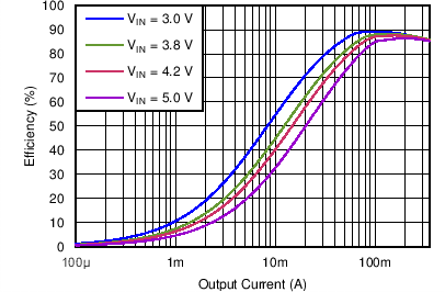
| DCDC1 | VO = 1.7 V |
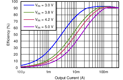
| DCDC2 | VO = 2.65 V |
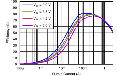
| DCDC3 | VO = 0.85 V |
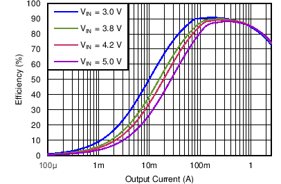
| DCDC3 | VO = 2.0 V |
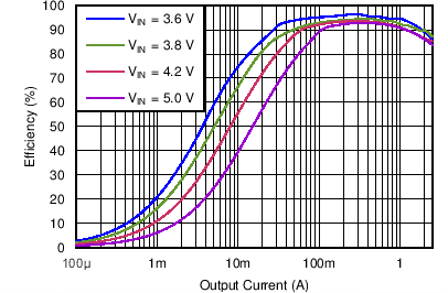
| DCDC3 | VO = 3.4 V |
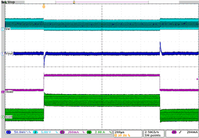
| IO= 30 mA to 270 mA | VO = 1.7 V | VI = 3.6 V |
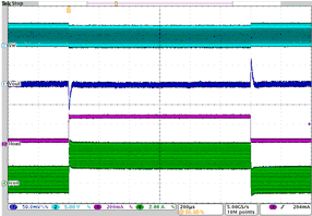
| IO= 30 mA to 270 mA | VO = 2.65 V | VI = 3.6 V |
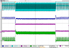
| IO= 100 mA to 900 mA | VO = 2.0 V | VI = 3.6 V |
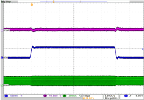
| VO= 1.7 V | VI = 3.6 V to 4.2 V | IO= 100 mA |
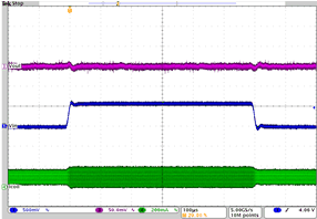
| VO= 2.65 V | VI = 3.6 V to 4.2 V | Load = 26.5 Ω at 100 mA |
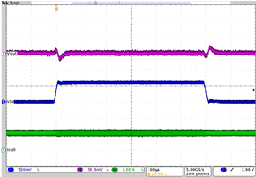
| VO = 2.0 V | VI= 3.6 V to 4.2 V | Load = 1.6 Ω at 1.25 A |
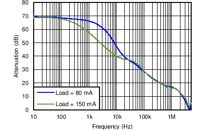
| VO = 1.7 V | VI= 3.6 V | Load = 80 mA, 150 mA |
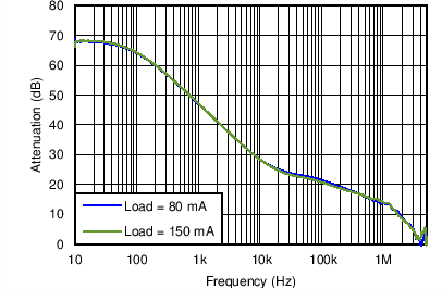
| VO = 2.0 V | VI= 3.6 V | Load = 80 mA, 150 mA |
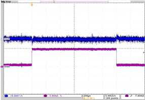
| IO= 1 mA to 9 mA | VO = 1.8 V | VI = 3.6 V |
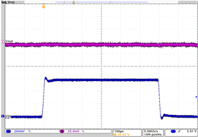
| VO = 1.8 V | VI= 3.6 V to 4.2 V | Load = 180 Ω at 10 mA |
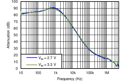
| VO = 1.8 V | Load = 10 mA | VI = 2.7 V, 3.3 V |
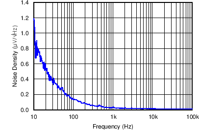
| VO = 1.8 V | Load = 180 Ω at 10 mA | VI= 3.6 V |
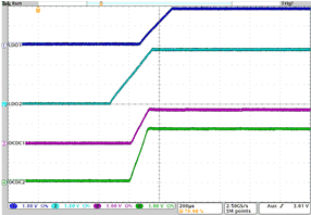
| VI= 3.6 V | Load = Open | |||
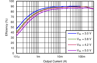
| DCDC1 | VO = 1.7 V |
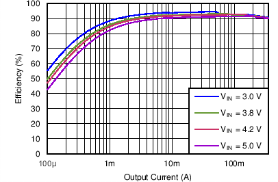
| DCDC2 | VO = 2.65 V |
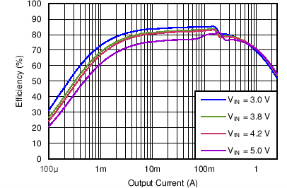
| DCDC3 | VO = 0.85 V |
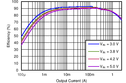
| DCDC3 | VO = 2.0 V |
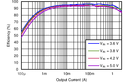
| DCDC3 | VO = 3.4 V |
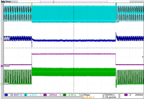
| IO= 30 mA to 270 mA | VO = 1.7 V | VI = 3.6 V |
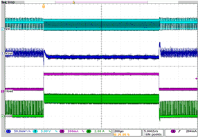
| IO= 30 mA to 270 mA | VO = 2.65 V | VI = 3.6 V |
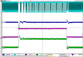
| IO= 200 mA to 1800 mA | VO = 3.4 V | VI = 3.8 V |
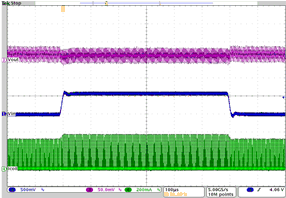
| VO= 1.7 V | VI = 3.6 V to 4.2 V | IO= 100 mA |
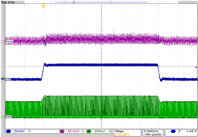
| VO= 2.65 V | VI = 3.6 V to 4.2 V | Load = 26.5 Ω at 100 mA |
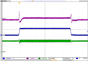
| VO = 3.4 V | VI= 3.6 V to 4.2 V | Load = 3.1 Ω at 1.1 A |
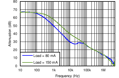
| VO = 2.65 V | VI= 3.6 V | Load = 80 mA, 150 mA |
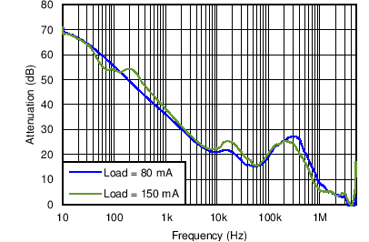
| VO = 3.4 V | VI= 3.6 V | Load = 80 mA, 150 mA |
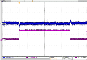
| IO= 1 mA to 9 mA | VO = 2.8 V | VI = 3.6 V |
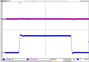
| VO = 2.8 V | VI= 3.6 V to 4.2 V | Load = 280 Ω at 10 mA |
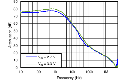
| VO = 2.8 V | Load = 10 mA | VI = 3.3 V, 3.6 V |
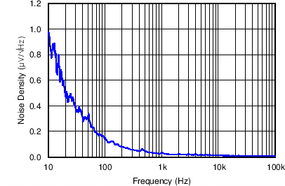
| VO = 2.8 V | Load = 280 Ω at 10 mA | VI= 3.6 V |