SLVSAI6A June 2011 – January 2016 TPS65735
PRODUCTION DATA.
- 1 Device Overview
- 2 Revision History
- 3 Terminal Configuration and Functions
- 4 Specifications
- 5 Detailed Description
- 6 Application and Implementation
- 7 Power Supply Recommendations
- 8 Layout
- 9 Device and Documentation Support
- 10Mechanical, Packaging, and Orderable Information
6 Application and Implementation
NOTE
Information in the following applications sections is not part of the TI component specification, and TI does not warrant its accuracy or completeness. TI’s customers are responsible for determining suitability of components for their purposes. Customers should validate and test their design implementation to confirm system functionality.
6.1 Application Information
This PMIC is designed specifically for active shutter 3D glasses.
6.2 Typical Application
6.2.1 Active Shutter 3D Glasses
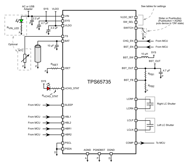 Figure 6-1 TPS65735 Applications Schematic
6.2.1.1 Design Requirements
The design parameters are located in Table 6-1.
Table 6-1 Design Parameters
| PARAMETER | EXAMPLE |
|---|---|
| Input Voltage, VIN | 3.7 to 6.4 V |
| Input Voltage, Vbat BAT | 2.5 to 6.4 V |
| Output Voltage, LDO VLDO | 2.2 (default) or 3.0 V |
| Output Voltage Boost, BST_OUT | 8 to 16 V, 10 V default |
| Charge Current Ichg=Kiset/Riset | 5 to 100 mA, 70 mA default |
| Input Voltage Low VIL
(BST_EN, CHG_EN, SW_SEL, VLDO, HBRx, HBLx) |
0.4 V |
| Input Voltage High VIH
(BST_EN, CHG_EN, SW_SEL, VLDO, HBRx, HBLx) |
1.2 V |
6.2.1.2 Detailed Design Procedure
6.2.1.2.1 Reducing System Quiescent Current (IQ)
This PMU device has been optimized for low power applications. If an even lower quiescent current is desired, the following circuit and configuration can be utilized to reduce system off / sleep quiescent current further. Please note that this will cause a slight efficiency drop to the overall system due to the addition of the resistance of the FET that has been added. With this circuit, achieving an IQ of less than 1 µA is possible. Please refer to the datasheet of the MCU used in the system to determine the system IQ that is possible.
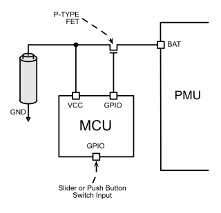 Figure 6-2 Reducing System IQ with Addition of a FET
Along with this system configuration, the MCU code must be written such that the MCU sits in the lowest power state that can support an interrupt on a GPIO from a switch (slider or push button). After a valid button press or switch action, the device can begin the power on sequence and open the FET in the previous figure (Figure 6-2). This will allow power flow into the PMU and the system can then operate normally.
6.2.1.2.2 Boost Converter Application Information
6.2.1.2.2.1 Setting Boost Output Voltage
To set the boost converter output voltage of this device, two external resistors that form a feedback network are required. The values recommended below (in Table 6-2) are given for a desired quiescent current of 5 µA when the boost is enabled and switching. See Figure 6-3 for the detail of the applications schematic that shows the boost feedback network and the resistor names used in the table below.
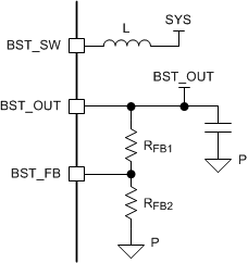 Figure 6-3 Boost Feedback Network Schematic
Table 6-2 Recommended RFB1 and RFB2 Values (for IQ(FB) = 5 µA)
| TARGETED VBST_OUT | RFB1(1) | RFB2(1) | ||
|---|---|---|---|---|
| 8 V | 1.3 MΩ | 240 kΩ | ||
| 10 V | 1.8 MΩ | 240 kΩ | ||
| 12 V | 2.2 MΩ | 240 kΩ | ||
| 14 V | 2.4 MΩ | 240 kΩ | ||
| 16 V | 3.0 MΩ | 240 kΩ | ||
These resistance values can also be calculated using the following information. To start, it is helpful to target a quiescent current through the boost feedback network while the device is operating (IQ(FB)). When the boost output voltage and this targeted quiescent current is known, the total feedback network resistance can be found.
The value for RFB2 can be found by using the boost feedback pin voltage (VFB = 1.2 V, see Section 4.6) and IQ(FB) using Equation 1:
To find RFB1, simply subtract the RFB2 from RFB(TOT) as shown in Equation 3.
6.2.1.2.2.2 Boost Inductor Selection
The selection of the boost inductor and output capacitor is very important to the performance of the boost converter. The boost has been designed for optimized operation when a 10 µH inductor is used. Smaller inductors, down to 4.7 µH, may be used but there will be a slight loss in overall operating efficiency. A few inductors that have been tested and found to give good performance can be found in the following list.
Recommended 10-µH inductors:
- TDK VLS201612ET-100M (10 µH, IMAX = 0.53 A, RDC = 0.85 Ω)
- Taiyo Yuden CBC2016B100M (10 µH, IMAX = 0.41 A, RDC = 0.82 Ω)
6.2.1.2.2.3 Boost Capacitor Selection
The recommended minimum value for the capacitor on the boost output, BST_OUT pin, is 4.7 µF. Values that are larger can be used with the measurable impact being a slight reduction in the boost converter output voltage ripple while values smaller than this will result in an increased boost output voltage ripple. Note that the voltage rating of the capacitor should be sized for the maximum expected voltage at the BST_OUT pin.
6.2.1.2.3 Bypassing Default Push-Button SWITCH Functionality
If the SWITCH pin functionality is not required to power on and off the device because of different system requirements (when the SWITCH timing requirements of system will be controlled by an external microcontroller), then the feature can be bypassed. The following diagram shows the connections required for this configuration, note that INT. I/O refers to an interruptible I/O on the microcontroller.
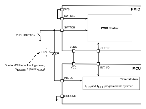 Figure 6-4 Bypassing Default TPS65735 Push Button SWITCH Timing
In a system where a different push-button SWITCH off timing is required, the SLEEP pin is used to control the power off of the device. After system power up, the MCU must force the SLEEP pin to a high state (VSLEEP > VIH(PMIC)). Once the SWITCH push-button is pressed to shut the system down, a timer in the MCU should be active and counting the desired tOFF time of the device. Once this tOFF time is detected, the MCU can assert the SLEEP signal to a logic low level (VSLEEP < VIL(PMIC)). It is on the falling edge of the SLEEP signal where the system will be powered off (see Figure 6-5).
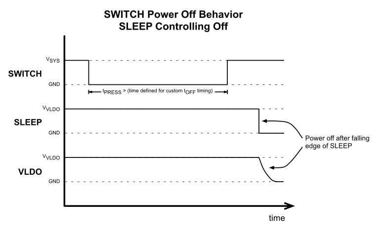 Figure 6-5 SWITCH Press and SLEEP Signal to Control System Power Off
6.2.1.3 Application Curves
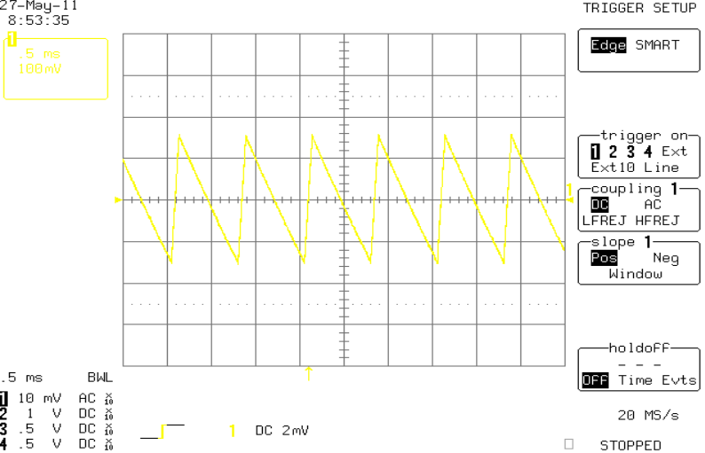
| Vbat = –3.2 V | 1-mA Load on Boost |
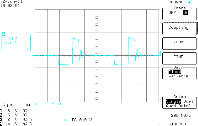
| Vbat = 3.6 V | No Load | 0.5 µs/div |