SLVSAI6A June 2011 – January 2016 TPS65735
PRODUCTION DATA.
- 1 Device Overview
- 2 Revision History
- 3 Terminal Configuration and Functions
- 4 Specifications
- 5 Detailed Description
- 6 Application and Implementation
- 7 Power Supply Recommendations
- 8 Layout
- 9 Device and Documentation Support
- 10Mechanical, Packaging, and Orderable Information
3 Terminal Configuration and Functions
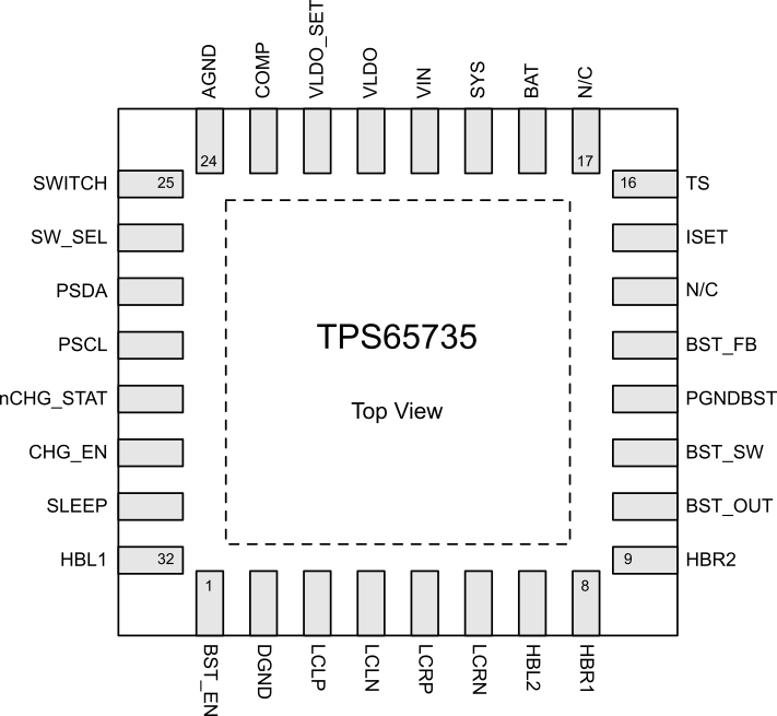
3.1 Pin Diagram

A. Pins 14 and 17 = N/C. No internal connection; connect to main system ground.
Figure 3-1 32-Pin RSN WQFN (Top View)
3.2 Pin Functions
Table 3-1 Pin Functions
| PIN | I/O | DESCRIPTION | |
|---|---|---|---|
| NO. | NAME | ||
| POWER MANAGEMENT CORE (PMIC) | |||
| 1 | BST_EN | I | Boost Enable Input from an MCU, High = Boost Enabled |
| 2 | DGND | — | Digital Ground |
| 3 | LCLP | O | H-Bridge Output for Left LC Shutter, Positive Terminal |
| 4 | LCLN | O | H-Bridge Output for Left LC Shutter, Negative Terminal |
| 5 | LCRP | O | H-Bridge Output for Right LC Shutter, Positive Terminal |
| 6 | LCRN | O | H-Bridge Output for Right LC Shutter, Negative Terminal |
| 7 | HBL2 | I | H-Bridge Input 2 for Left LC Shutter |
| 8 | HBR1 | I | H-Bridge Input 1 for Right LC Shutter |
| 9 | HBR2 | I | H-Bridge Input 2 for Right LC Shutter |
| 10 | BST_OUT | O | Boost Output |
| 11 | BST_SW | O | Boost Switch Node |
| 12 | PGNDBST | — | Boost Power Ground |
| 13 | BST_FB | I | Boost Feedback Node |
| 15 | ISET | I/O | Fast-Charge Current Setting Resistor |
| 16 | TS | I | Pin for 10-kΩ NTC Thermistor Connection FLOAT IF THERMISTOR / TS FUNCTION IS NOT USED |
| 18 | BAT | I/O | Charger Power Stage Output and Battery Voltage Sense Input |
| 19 | SYS | O | Output Terminal to System |
| 20 | VIN | I | AC or USB Adapter Input |
| 21 | VLDO | O | LDO Output |
| 22 | VLDO_SET | I | Sets LDO Output Voltage (see Table 5-2) |
| 23 | COMP | O | Scaled Battery Voltage for MCU Comparator or ADC Input (Battery Voltage Monitoring) DO NOT CONNECT IF COMP FUNCTION IS NOT USED |
| 24 | AGND | - | Analog Ground |
| 25 | SWITCH | I | Switch Input for Device Power On/Off |
| 26 | SW_SEL | I | Selects Type of Switch Connected to SWITCH Pin (see Table 5-6) |
| 27 | PSDA | I/O | I2C Data Pin (only used for TI debug and test) GROUND PIN IN APPLICATION |
| 28 | PSCL | I/O | I2C Clock Pin (only used for TI debug and test) GROUND PIN IN APPLICATION |
| 29 | nCHG_STAT | O | Open-drain Output, Charge Status Indication CONNECT TO GROUND IF FUNCTION IS NOT USED |
| 30 | CHG_EN | I | Charger Enable Input from an MCU, High = Boost Enabled |
| 31 | SLEEP | I/O | Sleep Enable Input from an MCU (edge triggered, only for system shutdown) |
| 32 | HBL1 | I | H-Bridge Input 1 for Left LC Shutter |
| MISCELLANEOUS AND PACKAGE | |||
| 14, 17 | N/C | — | All N/C should be connected to the main system ground. |
| 33 | Thermal PAD | — | There is an internal electrical connection between the exposed thermal pad and the AGND ground pin of the device. The thermal pad must be connected to the same potential as the AGND pin on the printed circuit board. Do not use the thermal pad as the primary ground input for the device. AGND pin must be connected to ground at all times. |