SLVSAF6A June 2011 – January 2016 TPS65835
PRODUCTION DATA.
- 1 Device Overview
- 2 Revision History
- 3 Terminal Configuration and Functions
- 4 Specifications
-
5 Detailed Description
- 5.1 Overview
- 5.2 Functional Block Diagram
- 5.3 Feature Description
- 5.4 Device Functional Modes
- 5.5
MSP430 CORE
- 5.5.1
MSP430 Electrical Characteristics
- 5.5.1.1 MSP430 Recommended Operating Conditions
- 5.5.1.2 Active Mode Supply Current Into VCC Excluding External Current
- 5.5.1.3 Typical Characteristics, Active Mode Supply Current (Into VCC)
- 5.5.1.4 Low-Power Mode Supply Currents (Into VCC) Excluding External Current
- 5.5.1.5 Typical Characteristics, Low-Power Mode Supply Currents
- 5.5.1.6 Schmitt-Trigger Inputs, Ports Px
- 5.5.1.7 Leakage Current, Ports Px
- 5.5.1.8 Outputs, Ports Px
- 5.5.1.9 Output Frequency, Ports Px
- 5.5.1.10 Typical Characteristics, Outputs
- 5.5.1.11 Pin-Oscillator Frequency - Ports Px
- 5.5.1.12 Typical Characteristics, Pin-Oscillator Frequency
- 5.5.1.13 POR/Brownout Reset (BOR)
- 5.5.1.14 Typical Characteristics, POR/Brownout Reset (BOR)
- 5.5.1.15 DCO Frequency
- 5.5.1.16 Calibrated DCO Frequencies, Tolerance
- 5.5.1.17 Wake-Up From Lower-Power Modes (LPM3/4)
- 5.5.1.18 Typical Characteristics, DCO Clock Wake-Up Time From LPM3/4
- 5.5.1.19 Crystal Oscillator, XT1, Low-Frequency Mode
- 5.5.1.20 Internal Very-Low-Power Low-Frequency Oscillator (VLO)
- 5.5.1.21 Timer_A
- 5.5.1.22 USCI (UART Mode)
- 5.5.1.23 USCI (SPI Master Mode)
- 5.5.1.24 USCI (SPI Slave Mode)
- 5.5.1.25 USCI (I2C Mode)
- 5.5.1.26 Comparator_A+
- 5.5.1.27 Typical Characteristics - Comparator_A+
- 5.5.1.28 10-Bit ADC, Power Supply and Input Range Conditions
- 5.5.1.29 10-Bit ADC, Built-In Voltage Reference
- 5.5.1.30 10-Bit ADC, External Reference
- 5.5.1.31 10-Bit ADC, Timing Parameters
- 5.5.1.32 10-Bit ADC, Linearity Parameters
- 5.5.1.33 10-Bit ADC, Temperature Sensor and Built-In VMID
- 5.5.1.34 Flash Memory
- 5.5.1.35 RAM
- 5.5.1.36 JTAG and Spy-Bi-Wire Interface
- 5.5.1.37 JTAG Fuse
- 5.5.2 MSP430 Core Operation
- 5.5.1
MSP430 Electrical Characteristics
- 6 Application and Implementation
- 7 Power Supply Recommendations
- 8 Layout
- 9 Device and Documentation Support
- 10Mechanical, Packaging, and Orderable Information
パッケージ・オプション
メカニカル・データ(パッケージ|ピン)
- RKP|40
サーマルパッド・メカニカル・データ
- RKP|40
発注情報
5 Detailed Description
5.1 Overview
The TPS65835 integrates a linear charger, Boost Converter and an MSP430 to create a PMIC for active shutter 3D glasses.
5.2 Functional Block Diagram
 Figure 5-1 TPS65835 Simplified Functional Block Diagram
5.3 Feature Description
5.3.1 System Operation
The system must complete the power up routine before it enters normal operating mode. The specific system operation depends on the setting defined by the state of the SW_SEL pin. The details of the system operation for each configuration of the SW_SEL pin are contained in this section.
5.3.1.1 System Power Up
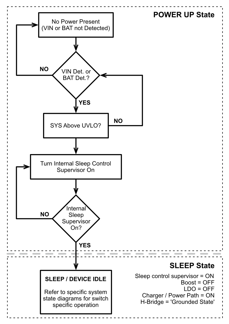 Figure 5-2 System Power Up State Diagram
5.3.1.2 System Operation Using Push Button Switch
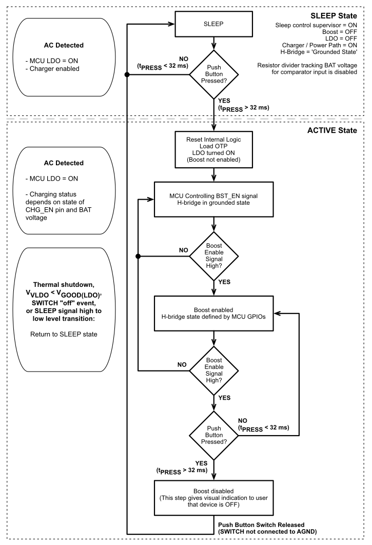 Figure 5-3 Push Button State Diagram
5.3.1.3 System Operation Using Slider Switch
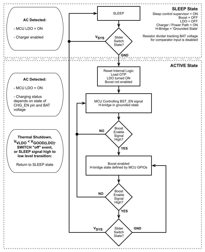 Figure 5-4 System Operation Using Slider Switch
5.3.2 Linear Charger Operation
This device has an integrated Li-Ion battery charger and system power path management feature targeted at space-limited portable applications. The architecture powers the system while simultaneously and independently charging the battery. This feature reduces the number of charge and discharge cycles on the battery, allows for proper charge termination, and enables the system to run with a defective or absent battery pack. It also allows instant system turn-on even with a totally discharged battery.
The input power source for charging the battery and running the system can be an AC adapter or USB port connected to the VIN pin as long as the input meets the device operating conditions outlined in this datasheet. The power-path management feature automatically reduces the charging current if the system load increases. Note that the charger input, VIN, has voltage protection up to 28 V.
5.3.2.1 Battery and TS Detection
To detect and determine between a good or damaged battery, the device checks for a short circuit on the BAT pin by sourcing IBAT(SC) to the battery and monitoring the voltage on the BAT pin. While sourcing this current if the BAT pin voltage exceeds VBAT(SC), a battery has been detected. If the voltage stays below the VBAT(SC) level, the battery is presumed to be damaged and not safe to charge.
The device will also check for the presence of a 10-kΩ NTC thermistor attached to the TS pin of the device. The check for the NTC thermistor on the TS pin is done much like the battery detection feature described previously. The voltage on the TS pin is compared against a defined level and if it is found to be above the threshold, the NTC thermistor is assumed to be disconnected or not used in the system. To reduce the system quiescent current, the NTC thermistor temperature sensing function is only enabled when the device is charging and when the thermistor has been detected.
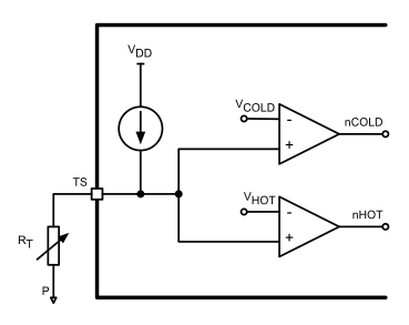 Figure 5-5 Thermistor Detection and Circuit
5.3.2.2 Battery Charging
The battery is charged in three phases: conditioning pre-charge, constant-current fast charge (current regulation), and a constant-voltage tapering (voltage regulation). In all charge phases, an internal control loop monitors the IC junction temperature and reduces the charge current if an internal temperature threshold is exceeded. Figure 5-6 shows what happens in each of the three charge phases:
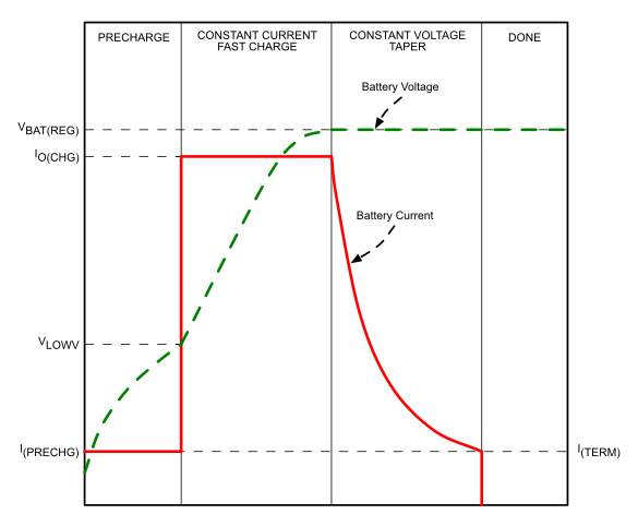 Figure 5-6 Battery Charge Phases
In the pre-charge phase, the battery is charged with the pre-charge current that is scaled to be 10% of the fast-charge current set by the resistor connected to the ISET pin. Once the battery voltage crosses the VLOWV threshold, the battery is charged with the fast-charge current (ICHG). As the battery voltage reaches VBAT(REG), the battery is held at a constant voltage of VBAT(REG) and the charge current tapers off as the battery approaches full charge. When the battery current reaches ITERM, the charger indicates charging is done by making the nCHG_STAT pin high impedance. Note that termination detection is disabled whenever the charge rate is reduced from the set point because of the actions of the thermal loop, the DPM loop, or the VIN(LOWV) loop.
5.3.2.2.1 Pre-charge
The value for the pre-charge current is set to be 10% of the charge current that is set by the external resistor, RISET. Pre-charge current is scaled to lower currents when the charger is in thermal regulation.
5.3.2.2.2 Charge Termination
In the fast charge state, once VBAT ≥ VBAT(REG), the charger enters constant voltage mode. In constant voltage mode, the charge current will taper until termination when the charge current falls below the I(TERM) threshold (typically 10% of the programmed fast charge current). Termination current is not scaled when the charger is in thermal regulation. When the charging is terminated, the nCHG_STAT pin will be high impedance (effectively turning off any LED that is connected to this pin).
5.3.2.2.3 Recharge
Once a charge cycle is complete and termination is reached, the battery voltage is monitored. If VBAT < VBAT(REG) - VRCH, the device determines if the battery has been removed. If the battery is still present, then the recharge cycle begins and will end when VBAT ≥ VBAT(REG).
5.3.2.2.4 Charge Timers
The charger in this device has internal safety timers for the pre-charge and fast charge phases to prevent potential damage to either the battery or the system. The default values for these timers are found as follows: Pre-charge timer = 0.5 hours (30 minutes) and Fast charge timer = 5 hours (300 minutes).
During the fast charge phase, the following events may increase the timer durations:
- The system load current activates the DPM loop which reduces the available charging current
- The input current is reduced because the input voltage has fallen to VIN(LOW)
- The device has entered thermal regulation because the IC junction temperature has exceeded TJ(REG)
During each of these events, the internal timers are slowed down proportionately to the reduction in charging current.
If the pre-charge timer expires before the battery voltage reaches VLOWV, the charger indicates a fault condition.
5.3.2.3 Charger Status (nCHG_STAT Pin)
The nCHG_STAT pin is used to indicate the charger status by an externally connected resistor and LED circuit. The pin is an open drain input and the internal switch is controlled by the logic inside of the charger. This pin may also be connected to a GPIO of the system MCU to indicate charging status. The table below details the status of the nCHG_STAT pin for various operating states of the charger.
Table 5-1 nCHG_STAT Functionality
| CHARGING STATUS | nCHG_STAT FET / LED | |||
|---|---|---|---|---|
| Pre-charge / Fast Charge / Charge Termination | ON | |||
| Recharge | OFF | |||
| OVP | OFF | |||
| SLEEP | OFF | |||
5.3.3 LDO Operation
The power management core has a low dropout linear regulator (LDO) with variable output voltage capability. This LDO is used for supplying the microcontroller and may be used to supply either an external IR or RF module, depending on system requirements. The LDO can supply a continuous current of up to 30 mA.
The output voltage (VVLDO) of the LDO is set by the state of the VLDO_SET pin. See Table 5-2 for details on setting the LDO output voltage.
Table 5-2 VLDO_SET Functionality
| VLDO_SET STATE | VLDO OUTPUT VOLTAGE (VVLDO) | |||
|---|---|---|---|---|
| Low (VLDO_SET < VIL(PMIC)) | 2.2 V | |||
| High (VLDO_SET > VIH(PMIC)) | 3.0 V | |||
5.3.3.1 LDO Internal Current Limit
The internal current limit feature helps protect the LDO regulator during fault conditions. During current limit, the output sources a fixed amount of current, defined in the Electrical Characteristics table. The voltage on the output in this stage can not be regulated and will be VOUT = ILIMIT × RLOAD. The pass transistor integrated into the LDO will dissipate power, (VIN - VOUT) × ILIMIT, until the device enters thermal shutdown. In thermal shutdown the device will enter the SLEEP / POWER OFF state which means that the LDO will then be disabled and shut off.
5.3.4 Boost Converter Operation
The boost converter in this device is designed for active shutter 3D glasses. This load is typically a light load where the average current is 2 mA or lower and the peak current out of a battery is limited in operation. This asynchronous boost converter operates with a minimum off time / maximum on time for the integrated low side switch, these values are specified in the Electrical Characteristics table of this datasheet.
The peak output voltage from the boost converter is adjustable and set by using an external resistor divider connected between BST_OUT pin, BST_FB pin, and ground. The peak output voltage is set by choosing resistors for the feedback network such that the voltage on the BST_FB pin is VREF(BST) = 1.2 V. See Section 6.2.1.2.1 for more information on calculating resistance values for this feedback network.
The efficiency curves for various input voltages over the typical 3D glasses load range (2 mA and lower) are shown below. All curves are for a target VOUT of 16 V. For output voltages less than 16 V, a higher efficiency at each operating input voltage should be expected. Note that efficiency is dependent upon the external boost feedback network resistance, the inductor used, and the type of load connected.
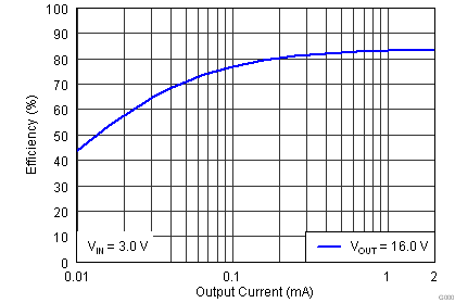
| VIN = 3.0 V | VOUT = 16 V |

| VIN = 4.2 V | VOUT = 16 V |
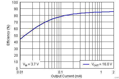
| VIN = 3.7 V | VOUT = 16 V |
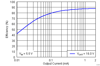
| VIN = 5.5 V | VOUT = 16 V |
5.3.4.1 Boost Thermal Shutdown
An internal thermal shutdown mode is implemented in the boost converter that shuts down the device if the typical junction temperature of 105°C is exceeded. If the device is in thermal shutdown mode, the main switch of the boost is open and the device enters the SLEEP / POWER OFF state.
5.3.4.2 Boost Load Disconnect
When the boost is disabled (BST_EN = LOW), the H-bridge is automatically placed into the OFF state. In the OFF state the high side H-bridge switches are open and the low side switches of the H-bridge are closed. The OFF state grounds and discharges the load, potentially prolonging the life of the LC shutters by eliminating any DC content (see Section 5.3.5.1 for more information regarding the H-bridge states). The disconnection of the load is done with the H-Bridge and can be seen in the next figure (Figure 5-11).
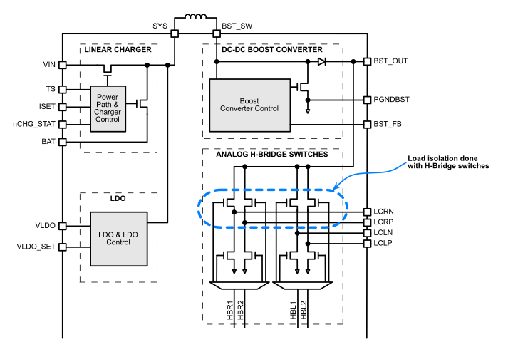 Figure 5-11 Boost Load Disconnect
An advantage to this topology for disconnecting the load is that the boost output capacitor is charged to approximately the SYS voltage level, specifically VSYS - VDIODE(BST), when the boost is disabled. This design ensures that there is not a large in-rush current into the boost output capacitor when the boost is enabled. The boost operation efficiency is also increased because there is no load disconnect switch in the boost output path. A load disconnect switch would decrease efficiency because of the resistance that it would introduce.
5.3.5 Full H-Bridge Analog Switches
The TPS65835 has two integrated full H-bridge analog switches that are connected to GPIO ports on the MSP430 and can be controlled by the MSP430 core for various system functions. There is an internal level shifter that manages the input signals to the H-Bridge switches.
5.3.5.1 H-Bridge Switch Control
The H-Bridge switches are controlled by the MSP430 core for system operation - specifically to control charge polarity on the LCD shutters. Depending on the state of the signals from the MSP430 core, the H-Bridge will be put into 4 different states. These states are:
- OPEN: All Switches Opened
- CHARGE+: Boost Output Voltage Present on Pins LCLP or LCRP
- CHARGE-: Boost Output Voltage Present on Pins LCLN or LCRN
- GROUNDED: High side switches are opened and low side switches are closed
If CHARGE+ state is followed by the CHARGE- state, the voltage across the capacitor connected to the H-Bridge output terminals will be reversed. The system automatically switches to the GROUNDED state when the boost is disabled by the BST_EN pin. For more details, see Section 5.3.1.
Table 5-3 H-Bridge States from Inputs
| HBx2 [HBL2 & HBR2] | HBx1 [HBL1 & HBR1] | H-Bridge STATE | ||
|---|---|---|---|---|
| 0 | 0 | OPEN | ||
| 0 | 1 | CHARGE + | ||
| 1 | 0 | CHARGE - | ||
| 1 | 1 | GROUNDED | ||
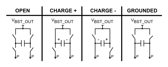 Figure 5-12 H-Bridge States
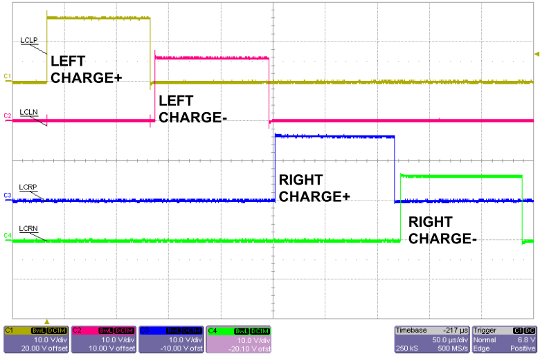 Figure 5-13 H-Bridge States from Oscilloscope
5.3.6 Power Management Core Control
The power management core is controlled with external pins that can set system behavior by their status along with internal connections to GPIOs from the MSP430. The internal connections to the GPIOs from the MSP430 can be modified through the code implemented in the MSP430.
5.3.6.1 SLEEP / Power Control Pin Function
The internal SLEEP signal between the power management device and the MSP430 can be used to control the power down behavior of the device. This has multiple practical applications such as a watchdog implementation for the communication between the sender (TV) and the receiver (3D glasses) or different required system on and off times; typically when the push-button press timing for an off event is a few seconds in length, programmable by software in the system MCU.
If there is a requirement that the push-button press for system on and off events are different, the SLEEP signal must be set to a logic high value (VSLEEP > VIH(PMIC)) upon system startup. This implementation allows the device to power down the system on the falling edge of the SLEEP signal
(when: VSLEEP < VIL(PMIC)).
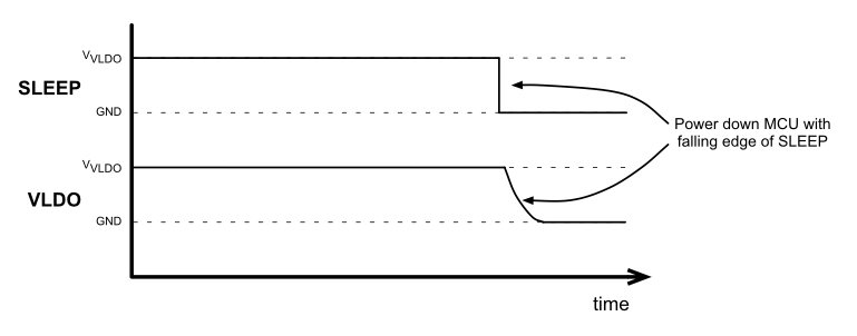 Figure 5-14 SLEEP Signal to Force System Power Off
5.3.6.2 COMP Pin Functionality
The COMP pin is used to output a scaled down voltage level related to the battery voltage for input to the comparator of the MSP430. Applications for this COMP feature could be to generate an interrupt on the MSP430 when the battery voltage drops under a threshold and the device can then be shut down or indicate to the end user with an LED that the battery requires charging.
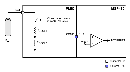 Figure 5-15 COMP Pin Internal Connection
Table 5-4 Scaling Resistors for COMP Pin Function (VVLDO = 2.2 V)
| SCALING RESISTORS FOR COMP PIN FUNCTION | VALUE | |||
|---|---|---|---|---|
| RBSCL1 | 3.0 MΩ | |||
| RBSCL2 | 2.36 MΩ | |||
Table 5-5 Scaling Resistors for COMP Pin Function (VVLDO = 3.0 V)
| SCALING RESISTORS FOR COMP PIN FUNCTION | VALUE | |||
|---|---|---|---|---|
| RBSCL1 | 3.0 MΩ | |||
| RBSCL2 | 2.48 MΩ | |||
Using the designed values in Table 5-4 or Table 5-5, the voltage on the COMP pin will be: VCOMP = 0.5 × VVLDO + 300 mV. This ensures that the COMP pin voltage will be close to half of the LDO output voltage plus the LDO dropout voltage of the device. The COMP pin can also be used as an input to ADC channel A0 of the integrated MSP430 microcontroller. This is useful if greater measurement accuracy or increased functionality is desired from this function.
5.3.6.3 SW_SEL Pin Functionality
The SW_SEL pin is used to select what type of switch is connected to the SWITCH pin of the device. Selection between a push-button and a slider switch can be made based on the state of this pin.
Table 5-6 SW_SEL Settings
| SW_SEL STATE | TYPE OF SWITCH SELECTED | |||
|---|---|---|---|---|
| Low (VSW_SEL < VIL(PMIC)) |
Slider Switch | |||
| High (VSW_SEL > VIH(PMIC)) |
Push-button | |||
When the push button switch type is selected, the device will debounce the SWITCH input with a 32-ms timer for both the ON and OFF events and either power on or off the device. Using the push-button switch function, the ON and OFF timings are equal; tON = tOFF. If the system requirements are such that the on and off timings should be different, tON ≠ tOFF, then refer to the following section for the correct system setup: Section 6.2.1.2.2.When the slider switch operation is selected, the SWITCH pin must be externally pulled up to the SYS voltage with a resistor and the output connected to the slider switch. When the SWITCH pin is pulled to ground, the device will turn on and enter the power up sequence.
5.3.6.4 SWITCH Pin
The SWITCH pin behavior is defined by the SW_SEL pin (Section 5.3.6.3) which defines the type of switch that is connected to the system; either a slider switch or push-button.
5.3.6.5 Slider Switch Behavior
If a slider switch is connected in the system then the system power state and VLDO output (which powers the internal MSP430) is defined by the state of the slider switch. If the slider is in the off position than the SWITCH pin should be connected to the SYS pin. If the slider is in the on position than the SWITCH pin should be connected to ground. Figure 5-16 details the system operation using the slider switch configuration.
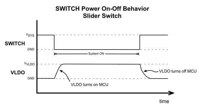 Figure 5-16 SWITCH, Slider Power On-Off Behavior
5.3.6.6 Push-Button Switch Behavior
The system is powered on or off by a push-button press after a press that is greater than 32 ms. The following figures (Figure 5-17 and Figure 5-18) show the system behavior and the expected VLDO output during the normal push-button operation where the ON and OFF press timings are the same value,
tON = tOFF.
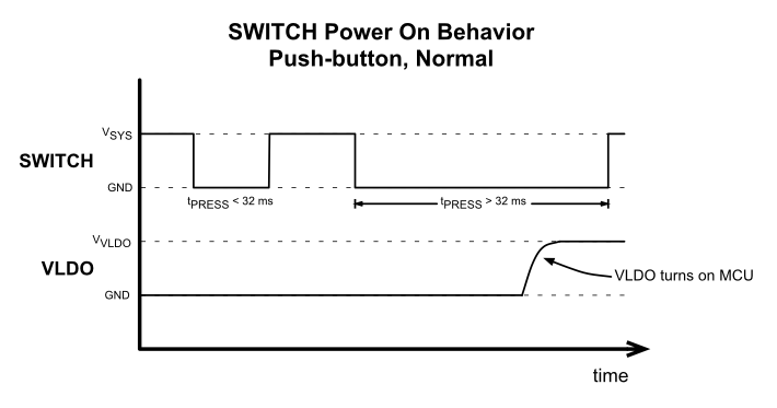 Figure 5-17 SWITCH, Push-button Power On Behavior
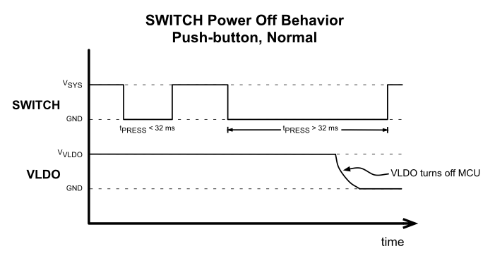 Figure 5-18 SWITCH, Push-Button Power Off Behavior
5.4 Device Functional Modes
5.4.1 SLEEP State
If the device is in the SLEEP State or Device IDLE mode, the Sleep control supervisor and the battery charger/power path remain active. The Boost and LDO are disabled.
5.4.2 NORMAL Operating Mode
Once the system completes the power up routine, it enters the normal operating mode. The specific system operation is set by the SW_SEL pin.
5.5 MSP430 CORE
5.5.1 MSP430 Electrical Characteristics
5.5.1.1 MSP430 Recommended Operating Conditions
| MIN | NOM | MAX | UNIT | |||
|---|---|---|---|---|---|---|
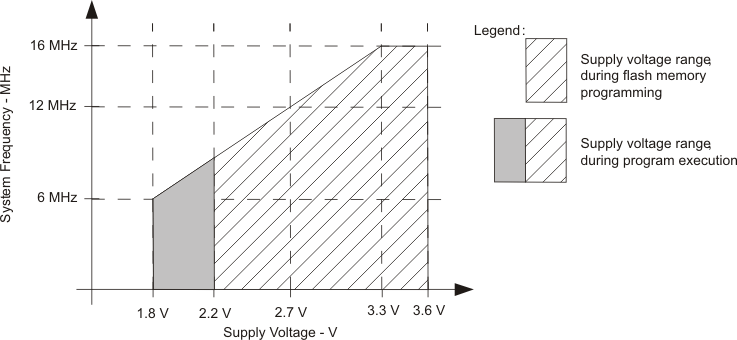
| VCC | Supply voltage | During program execution | 1.8 | 3.6 | V | |
| During flash programming/erase | 2.2 | 3.6 | ||||
| VSS | Supply voltage | 0 | V | |||
| fSYSTEM | Processor frequency (maximum MCLK frequency using the USART module)(1)(2) | VCC = 1.8 V, Duty cycle = 50% ± 10% |
dc | 6 | MHz | |
| VCC = 2.7 V, Duty cycle = 50% ± 10% |
dc | 12 | ||||
| VCC = 3.3 V, Duty cycle = 50% ± 10% |
dc | 16 | ||||
NOTE:
Minimum processor frequency is defined by system clock. Flash program or erase operations require a minimum VCC of 2.2 V.5.5.1.2 Active Mode Supply Current Into VCC Excluding External Current
over recommended ranges of supply voltage and operating free-air temperature (unless otherwise noted)(1)(2)| PARAMETER | TEST CONDITIONS | TA | VCC | MIN | TYP | MAX | UNIT | |
|---|---|---|---|---|---|---|---|---|
| IAM,1MHz | Active mode (AM) current at 1 MHz | fDCO = fMCLK = fSMCLK = 1 MHz, fACLK = 0 Hz, Program executes in flash, BCSCTL1 = CALBC1_1MHZ, DCOCTL = CALDCO_1MHZ, CPUOFF = 0, SCG0 = 0, SCG1 = 0, OSCOFF = 0 |
2.2 V | 230 | µA | |||
| 3 V | 330 | 420 | ||||||
5.5.1.3 Typical Characteristics, Active Mode Supply Current (Into VCC)
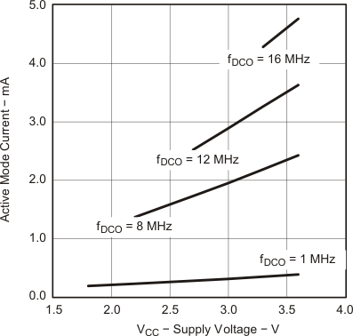 Figure 5-20 Active Mode Current vs VCC, TA = 25°C
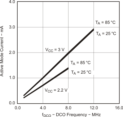 Figure 5-21 Active Mode Current vs DCO Frequency
5.5.1.4 Low-Power Mode Supply Currents (Into VCC) Excluding External Current
over recommended ranges of supply voltage and operating free-air temperature (unless otherwise noted)(1) (2)| PARAMETER | TEST CONDITIONS | TA | VCC | MIN | TYP | MAX | UNIT | |
|---|---|---|---|---|---|---|---|---|
| ILPM0,1MHz | Low-power mode 0 (LPM0) current(3) | fMCLK = 0 MHz, fSMCLK = fDCO = 1 MHz, fACLK = 32768 Hz, BCSCTL1 = CALBC1_1MHZ, DCOCTL = CALDCO_1MHZ, CPUOFF = 1, SCG0 = 0, SCG1 = 0, OSCOFF = 0 |
25°C | 2.2 V | 56 | µA | ||
| ILPM2 | Low-power mode 2 (LPM2) current(4) | fMCLK = fSMCLK = 0 MHz, fDCO = 1 MHz, fACLK = 32768 Hz, BCSCTL1 = CALBC1_1MHZ, DCOCTL = CALDCO_1MHZ, CPUOFF = 1, SCG0 = 0, SCG1 = 1, OSCOFF = 0 |
25°C | 2.2 V | 22 | µA | ||
| ILPM3,LFXT1 | Low-power mode 3 (LPM3) current(4) | fDCO = fMCLK = fSMCLK = 0 MHz, fACLK = 32768 Hz, CPUOFF = 1, SCG0 = 1, SCG1 = 1, OSCOFF = 0 |
25°C | 2.2 V | 0.7 | 1.5 | µA | |
| ILPM3,VLO | Low-power mode 3 current, (LPM3)(4) | fDCO = fMCLK = fSMCLK = 0 MHz, fACLK from internal LF oscillator (VLO), CPUOFF = 1, SCG0 = 1, SCG1 = 1, OSCOFF = 0 |
25°C | 2.2 V | 0.5 | 0.7 | µA | |
| ILPM4 | Low-power mode 4 (LPM4) current(5) | fDCO = fMCLK = fSMCLK = 0 MHz, fACLK = 0 Hz, CPUOFF = 1, SCG0 = 1, SCG1 = 1, OSCOFF = 1 |
25°C | 2.2 V | 0.1 | 0.5 | µA | |
| 85°C | 0.8 | 1.7 | ||||||
- All inputs are tied to 0 V or to VCC. Outputs do not source or sink any current.
- The currents are characterized with a Micro Crystal CC4V-T1A SMD crystal with a load capacitance of 9 pF. The internal and external load capacitance is chosen to closely match the required 9 pF.
- Current for brownout and WDT clocked by SMCLK included.
- Current for brownout and WDT clocked by ACLK included.
- Current for brownout included.
5.5.1.5 Typical Characteristics, Low-Power Mode Supply Currents
over recommended ranges of supply voltage and operating free-air temperature (unless otherwise noted)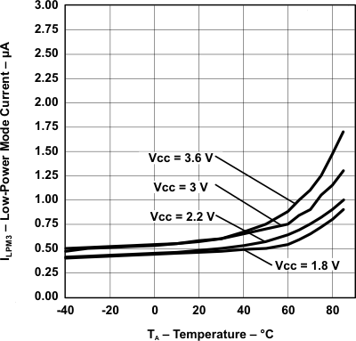 Figure 5-22 LPM3 Current vs Temperature
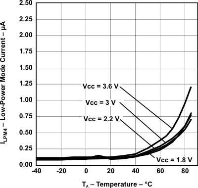 Figure 5-23 LPM4 Current vs Temperature
5.5.1.6 Schmitt-Trigger Inputs, Ports Px
over recommended ranges of supply voltage and operating free-air temperature (unless otherwise noted)| PARAMETER | TEST CONDITIONS | VCC | MIN | TYP | MAX | UNIT | |
|---|---|---|---|---|---|---|---|
| VIT+ | Positive-going input threshold voltage | 0.45 VCC | 0.75 VCC | V | |||
| 3 V | 1.35 | 2.25 | |||||
| VIT– | Negative-going input threshold voltage | 0.25 VCC | 0.55 VCC | V | |||
| 3 V | 0.75 | 1.65 | |||||
| Vhys | Input voltage hysteresis (VIT+ – VIT–) | 3 V | 0.3 | 1 | V | ||
| RPull | Pull-up/pull-down resistor | For pull-up: VIN = VSS
For pull-down: VIN = VCC |
3 V | 20 | 35 | 50 | kΩ |
| CI | Input capacitance | VIN = VSS or VCC | 5 | pF | |||
5.5.1.7 Leakage Current, Ports Px
over recommended ranges of supply voltage and operating free-air temperature (unless otherwise noted)| PARAMETER | TEST CONDITIONS | VCC | MIN | MAX | UNIT | |
|---|---|---|---|---|---|---|
| Ilkg(Px.y) | High-impedance leakage current | (1) (2) | 3 V | ±50 | nA | |
5.5.1.8 Outputs, Ports Px
over recommended ranges of supply voltage and operating free-air temperature (unless otherwise noted)| PARAMETER | TEST CONDITIONS | VCC | MIN | TYP | MAX | UNIT | |
|---|---|---|---|---|---|---|---|
| VOH | High-level output voltage | I(OHmax) = –6 mA(1) | 3 V | VCC – 0.3 | V | ||
| VOL | Low-level output voltage | I(OLmax) = 6 mA(1) | 3 V | VSS + 0.3 | V | ||
5.5.1.9 Output Frequency, Ports Px
over recommended ranges of supply voltage and operating free-air temperature (unless otherwise noted)| PARAMETER | TEST CONDITIONS | VCC | MIN | TYP | MAX | UNIT | |
|---|---|---|---|---|---|---|---|
| fPx.y | Port output frequency (with load) | Px.y, CL = 20 pF, RL = 1 kΩ(1) (2) | 3 V | 12 | MHz | ||
| fPort_CLK | Clock output frequency | Px.y, CL = 20 pF(2) | 3 V | 16 | MHz | ||
5.5.1.10 Typical Characteristics, Outputs
over recommended ranges of supply voltage and operating free-air temperature (unless otherwise noted)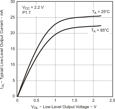 Figure 5-24 Typical Low-Level Output Current vs Low-Level Output Voltage
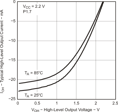 Figure 5-26 Typical High-Level Output Current vs High-Level Output Voltage
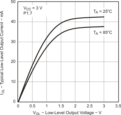 Figure 5-25 Typical Low-Level Output Current vs Low-Level Output Voltage
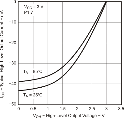 Figure 5-27 Typical High-Level Output Current vs High-Level Output Voltage
5.5.1.11 Pin-Oscillator Frequency – Ports Px
over recommended ranges of supply voltage and operating free-air temperature (unless otherwise noted)| PARAMETER | TEST CONDITIONS | VCC | MIN | TYP | MAX | UNIT | |
|---|---|---|---|---|---|---|---|
| foP1.x | Port output oscillation frequency | P1.y, CL = 10 pF, RL = 100 kΩ(1)(2) | 3 V | 1400 | kHz | ||
| P1.y, CL = 20 pF, RL = 100 kΩ(1)(2) | 900 | ||||||
| foP2.x | Port output oscillation frequency | P2.0 to P2.5, CL = 10 pF, RL = 100 kΩ(1)(2) | 1800 | kHz | |||
| P2.0 to P2.5, CL = 20 pF, RL = 100 kΩ(1)(2) | 3 V | 1000 | |||||
| foP2.6/7 | Port output oscillation frequency | P2.6 and P2.7, CL = 20 pF, RL = 100 kΩ(1)(2) | 3 V | 700 | kHz | ||
| foP3.x | Port output oscillation frequency | P3.y, CL = 10 pF, RL = 100 kΩ(1)(2) | 1800 | kHz | |||
| P3.y, CL = 20 pF, RL = 100 kΩ(1)(2) | 1000 | ||||||
5.5.1.12 Typical Characteristics, Pin-Oscillator Frequency
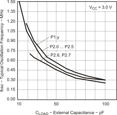
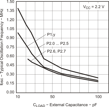
5.5.1.13 POR/Brownout Reset (BOR)(1)
over recommended ranges of supply voltage and operating free-air temperature (unless otherwise noted)| PARAMETER | TEST CONDITIONS | VCC | MIN | TYP | MAX | UNIT | |
|---|---|---|---|---|---|---|---|
| VCC(start) | See Figure 5-30 | dVCC/dt ≤ 3 V/s | 0.7 × V(B_IT--) | V | |||
| V(B_IT–) | See Figure 5-30 through Figure 5-32 | dVCC/dt ≤ 3 V/s | 1.35 | V | |||
| Vhys(B_IT–) | See Figure 5-30 | dVCC/dt ≤ 3 V/s | 140 | mV | |||
| td(BOR) | See Figure 5-30 | 2000 | µs | ||||
| t(reset) | Pulse length needed at RST/NMI pin to accepted reset internally | 2.2 V | 2 | µs | |||
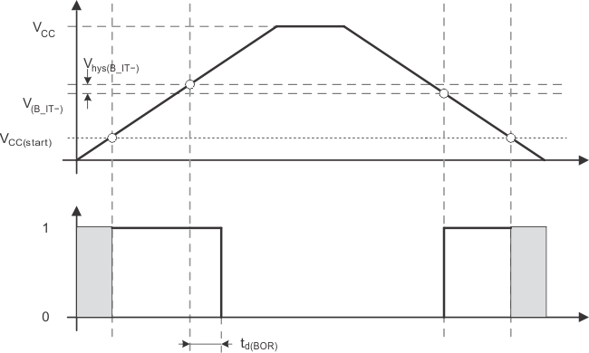 Figure 5-30 POR/Brownout Reset (BOR) vs Supply Voltage
5.5.1.14 Typical Characteristics, POR/Brownout Reset (BOR)
 Figure 5-31 VCC(drop) Level With a Square Voltage Drop to Generate a POR/Brownout Signal
 Figure 5-32 VCC(drop) Level With a Triangle Voltage Drop to Generate a POR/Brownout Signal
5.5.1.15 DCO Frequency
over recommended ranges of supply voltage and operating free-air temperature (unless otherwise noted)| PARAMETER | TEST CONDITIONS | VCC | MIN | TYP | MAX | UNIT | |
|---|---|---|---|---|---|---|---|
| VCC | Supply voltage | RSELx < 14 | 1.8 | 3.6 | V | ||
| RSELx = 14 | 2.2 | 3.6 | |||||
| RSELx = 15 | 3 | 3.6 | |||||
| fDCO(0,0) | DCO frequency (0, 0) | RSELx = 0, DCOx = 0, MODx = 0 | 3 V | 0.06 | 0.14 | MHz | |
| fDCO(0,3) | DCO frequency (0, 3) | RSELx = 0, DCOx = 3, MODx = 0 | 3 V | 0.07 | 0.17 | MHz | |
| fDCO(1,3) | DCO frequency (1, 3) | RSELx = 1, DCOx = 3, MODx = 0 | 3 V | 0.15 | MHz | ||
| fDCO(2,3) | DCO frequency (2, 3) | RSELx = 2, DCOx = 3, MODx = 0 | 3 V | 0.21 | MHz | ||
| fDCO(3,3) | DCO frequency (3, 3) | RSELx = 3, DCOx = 3, MODx = 0 | 3 V | 0.30 | MHz | ||
| fDCO(4,3) | DCO frequency (4, 3) | RSELx = 4, DCOx = 3, MODx = 0 | 3 V | 0.41 | MHz | ||
| fDCO(5,3) | DCO frequency (5, 3) | RSELx = 5, DCOx = 3, MODx = 0 | 3 V | 0.58 | MHz | ||
| fDCO(6,3) | DCO frequency (6, 3) | RSELx = 6, DCOx = 3, MODx = 0 | 3 V | 0.54 | 1.06 | MHz | |
| fDCO(7,3) | DCO frequency (7, 3) | RSELx = 7, DCOx = 3, MODx = 0 | 3 V | 0.80 | 1.50 | MHz | |
| fDCO(8,3) | DCO frequency (8, 3) | RSELx = 8, DCOx = 3, MODx = 0 | 3 V | 1.6 | MHz | ||
| fDCO(9,3) | DCO frequency (9, 3) | RSELx = 9, DCOx = 3, MODx = 0 | 3 V | 2.3 | MHz | ||
| fDCO(10,3) | DCO frequency (10, 3) | RSELx = 10, DCOx = 3, MODx = 0 | 3 V | 3.4 | MHz | ||
| fDCO(11,3) | DCO frequency (11, 3) | RSELx = 11, DCOx = 3, MODx = 0 | 3 V | 4.25 | MHz | ||
| fDCO(12,3) | DCO frequency (12, 3) | RSELx = 12, DCOx = 3, MODx = 0 | 3 V | 4.30 | 7.30 | MHz | |
| fDCO(13,3) | DCO frequency (13, 3) | RSELx = 13, DCOx = 3, MODx = 0 | 3 V | 6.00 | 7.8 | 9.60 | MHz |
| fDCO(14,3) | DCO frequency (14, 3) | RSELx = 14, DCOx = 3, MODx = 0 | 3 V | 8.60 | 13.9 | MHz | |
| fDCO(15,3) | DCO frequency (15, 3) | RSELx = 15, DCOx = 3, MODx = 0 | 3 V | 12.0 | 18.5 | MHz | |
| fDCO(15,7) | DCO frequency (15, 7) | RSELx = 15, DCOx = 7, MODx = 0 | 3 V | 16.0 | 26.0 | MHz | |
| SRSEL | Frequency step between range RSEL and RSEL+1 | SRSEL = fDCO(RSEL+1,DCO)/fDCO(RSEL,DCO) | 3 V | 1.35 | ratio | ||
| SDCO | Frequency step between tap DCO and DCO+1 | SDCO = fDCO(RSEL,DCO+1)/fDCO(RSEL,DCO) | 3 V | 1.08 | ratio | ||
| Duty cycle | Measured at SMCLK output | 3 V | 50% | ||||
5.5.1.16 Calibrated DCO Frequencies, Tolerance
over recommended ranges of supply voltage and operating free-air temperature (unless otherwise noted)| PARAMETER | TEST CONDITIONS | TA | VCC | MIN | TYP | MAX | UNIT |
|---|---|---|---|---|---|---|---|
| 1-MHz tolerance over temperature(1) | BCSCTL1 = CALBC1_1MHZ, DCOCTL = CALDCO_1MHZ, calibrated at 30°C and 3 V |
0°C to 85°C | 3 V | –3% | ±0.5% | 3% | |
| 1-MHz tolerance over VCC | BCSCTL1 = CALBC1_1MHZ, DCOCTL = CALDCO_1MHZ, calibrated at 30°C and 3 V |
30°C | 1.8 V to 3.6 V | –3% | ±2% | 3% | |
| 1-MHz tolerance overall | BCSCTL1 = CALBC1_1MHZ, DCOCTL = CALDCO_1MHZ, calibrated at 30°C and 3 V |
–40°C to 85°C | 1.8 V to 3.6 V | –6% | ±3% | 6% | |
| 8-MHz tolerance over temperature(1) | BCSCTL1 = CALBC1_8MHZ, DCOCTL = CALDCO_8MHZ, calibrated at 30°C and 3 V |
0°C to 85°C | 3 V | –3% | ±0.5% | 3% | |
| 8-MHz tolerance over VCC | BCSCTL1 = CALBC1_8MHZ, DCOCTL = CALDCO_8MHZ, calibrated at 30°C and 3 V |
30°C | 2.2 V to 3.6 V | –3% | ±2% | 3% | |
| 8-MHz tolerance overall | BCSCTL1 = CALBC1_8MHZ, DCOCTL = CALDCO_8MHZ, calibrated at 30°C and 3 V |
–40°C to 85°C | 2.2 V to 3.6 V | –6% | ±3% | 6% | |
| 12-MHz tolerance over temperature(1) | BCSCTL1 = CALBC1_12MHZ, DCOCTL = CALDCO_12MHZ, calibrated at 30°C and 3 V |
0°C to 85°C | 3 V | –3% | ±0.5% | 3% | |
| 12-MHz tolerance over VCC | BCSCTL1 = CALBC1_12MHZ, DCOCTL = CALDCO_12MHZ, calibrated at 30°C and 3 V |
30°C | 2.7 V to 3.6 V | –3% | ±2% | 3% | |
| 12-MHz tolerance overall | BCSCTL1 = CALBC1_12MHZ, DCOCTL = CALDCO_12MHZ, calibrated at 30°C and 3 V |
–40°C to 85°C | 2.7 V to 3.6 V | –6% | ±3% | 6% | |
| 16-MHz tolerance over temperature(1) | BCSCTL1 = CALBC1_16MHZ, DCOCTL = CALDCO_16MHZ, calibrated at 30°C and 3 V |
0°C to 85°C | 3 V | –3% | ±0.5% | 3% | |
| 16-MHz tolerance over VCC | BCSCTL1 = CALBC1_16MHZ, DCOCTL = CALDCO_16MHZ, calibrated at 30°C and 3 V |
30°C | 3.3 V to 3.6 V | –3% | ±2% | 3% | |
| 16-MHz tolerance overall | BCSCTL1 = CALBC1_16MHZ, DCOCTL = CALDCO_16MHZ, calibrated at 30°C and 3 V |
–40°C to 85°C | 3.3 V to 3.6 V | –6% | ±3% | 6% |
5.5.1.17 Wake-Up From Lower-Power Modes (LPM3/4)
over recommended ranges of supply voltage and operating free-air temperature (unless otherwise noted)| PARAMETER | TEST CONDITIONS | VCC | MIN | TYP | MAX | UNIT | |
|---|---|---|---|---|---|---|---|
| tDCO,LPM3/4 | DCO clock wake-up time from LPM3/4(1) | BCSCTL1 = CALBC1_1MHz, DCOCTL = CALDCO_1MHz | 3 V | 1.5 | µs | ||
| tCPU,LPM3/4 | CPU wake-up time from LPM3/4(2) | 1/fMCLK + tClock,LPM3/4 |
|||||
5.5.1.18 Typical Characteristics, DCO Clock Wake-Up Time From LPM3/4
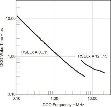 Figure 5-33 DCO Wake-Up Time From LPM3 vs DCO Frequency
5.5.1.19 Crystal Oscillator, XT1, Low-Frequency Mode
over recommended ranges of supply voltage and operating free-air temperature (unless otherwise noted)| PARAMETER(1) | TEST CONDITIONS | VCC | MIN | TYP | MAX | UNIT | |
|---|---|---|---|---|---|---|---|
| fLFXT1,LF | LFXT1 oscillator crystal frequency, LF mode 0, 1 | XTS = 0, LFXT1Sx = 0 or 1 | 1.8 V to 3.6 V | 32768 | Hz | ||
| fLFXT1,LF,logic | LFXT1 oscillator logic level square wave input frequency, LF mode | XTS = 0, XCAPx = 0, LFXT1Sx = 3 | 1.8 V to 3.6 V | 10000 | 32768 | 50000 | Hz |
| OALF | Oscillation allowance for LF crystals | XTS = 0, LFXT1Sx = 0, fLFXT1,LF = 32768 Hz, CL,eff = 6 pF |
500 | kΩ | |||
| XTS = 0, LFXT1Sx = 0, fLFXT1,LF = 32768 Hz, CL,eff = 12 pF |
200 | ||||||
| CL,eff | Integrated effective load capacitance, LF mode(2) | XTS = 0, XCAPx = 0 | 1 | pF | |||
| XTS = 0, XCAPx = 1 | 5.5 | ||||||
| XTS = 0, XCAPx = 2 | 8.5 | ||||||
| XTS = 0, XCAPx = 3 | 11 | ||||||
| Duty cycle | LF mode | XTS = 0, Measured at P2.0/ACLK, fLFXT1,LF = 32768 Hz |
2.2 V | 30% | 50% | 70% | |
| fFault,LF | Oscillator fault frequency, LF mode(4) | XTS = 0, XCAPx = 0, LFXT1Sx = 3(3) | 2.2 V | 10 | 10000 | Hz | |
- Keep the trace between the device and the crystal as short as possible.
- Design a good ground plane around the oscillator pins.
- Prevent crosstalk from other clock or data lines into oscillator pins XIN and XOUT.
- Avoid running PCB traces underneath or adjacent to the XIN and XOUT pins.
- Use assembly materials and praxis to avoid any parasitic load on the oscillator XIN and XOUT pins.
- If conformal coating is used, ensure that it does not induce capacitive/resistive leakage between the oscillator pins.
- Do not route the XOUT line to the JTAG header to support the serial programming adapter as shown in other documentation. This signal is no longer required for the serial programming adapter.
5.5.1.20 Internal Very-Low-Power Low-Frequency Oscillator (VLO)
over recommended ranges of supply voltage and operating free-air temperature (unless otherwise noted)| PARAMETER | TA | VCC | MIN | TYP | MAX | UNIT | |
|---|---|---|---|---|---|---|---|
| fVLO | VLO frequency | –40°C to 85°C | 3 V | 4 | 12 | 20 | kHz |
| dfVLO/dT | VLO frequency temperature drift | –40°C to 85°C | 3 V | 0.5 | %/°C | ||
| dfVLO/dVCC | VLO frequency supply voltage drift | 25°C | 1.8 V to 3.6 V | 4 | %/V | ||
5.5.1.21 Timer_A
over recommended ranges of supply voltage and operating free-air temperature (unless otherwise noted)| PARAMETER | TEST CONDITIONS | VCC | MIN | TYP | MAX | UNIT | |
|---|---|---|---|---|---|---|---|
| fTA | Timer_A input clock frequency | SMCLK, duty cycle = 50% ± 10% | fSYSTEM | MHz | |||
| tTA,cap | Timer_A capture timing | TA0, TA1 | 3 V | 20 | ns | ||
5.5.1.22 USCI (UART Mode)
over recommended ranges of supply voltage and operating free-air temperature (unless otherwise noted)| PARAMETER | TEST CONDITIONS | VCC | MIN | TYP | MAX | UNIT | |
|---|---|---|---|---|---|---|---|
| fUSCI | USCI input clock frequency | SMCLK, duty cycle = 50% ± 10% | fSYSTEM | MHz | |||
| fmax,BITCLK | Maximum BITCLK clock frequency (equals baudrate in MBaud)(1) | 3 V | 2 | MHz | |||
| tτ | UART receive deglitch time(2) | 3 V | 50 | 100 | 600 | ns | |
5.5.1.23 USCI (SPI Master Mode)
over recommended ranges of supply voltage and operating free-air temperature (unless otherwise noted) (see Figure 5-34 and Figure 5-35)| PARAMETER | TEST CONDITIONS | VCC | MIN | TYP | MAX | UNIT | |
|---|---|---|---|---|---|---|---|
| fUSCI | USCI input clock frequency | SMCLK, duty cycle = 50% ± 10% | fSYSTEM | MHz | |||
| tSU,MI | SOMI input data setup time | 3 V | 75 | ns | |||
| tHD,MI | SOMI input data hold time | 3 V | 0 | ns | |||
| tVALID,MO | SIMO output data valid time | UCLK edge to SIMO valid, CL = 20 pF | 3 V | 20 | ns | ||
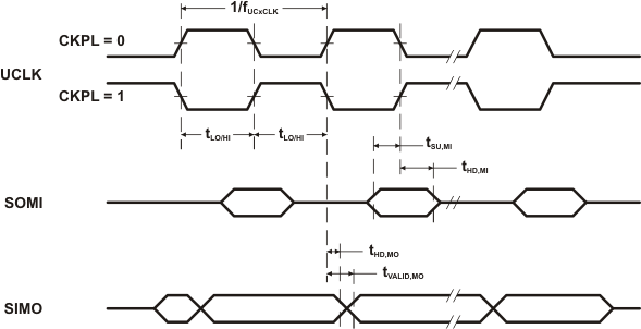 Figure 5-34 SPI Master Mode, CKPH = 0
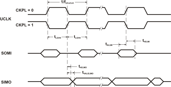 Figure 5-35 SPI Master Mode, CKPH = 1
5.5.1.24 USCI (SPI Slave Mode)
over recommended ranges of supply voltage and operating free-air temperature (unless otherwise noted) (see Figure 5-36 and Figure 5-37)| PARAMETER | TEST CONDITIONS | VCC | MIN | TYP | MAX | UNIT | |
|---|---|---|---|---|---|---|---|
| tSTE,LEAD | STE lead time, STE low to clock | 3 V | 50 | ns | |||
| tSTE,LAG | STE lag time, Last clock to STE high | 3 V | 10 | ns | |||
| tSTE,ACC | STE access time, STE low to SOMI data out | 3 V | 50 | ns | |||
| tSTE,DIS | STE disable time, STE high to SOMI high impedance | 3 V | 50 | ns | |||
| tSU,SI | SIMO input data setup time | 3 V | 15 | ns | |||
| tHD,SI | SIMO input data hold time | 3 V | 10 | ns | |||
| tVALID,SO | SOMI output data valid time | UCLK edge to SOMI valid, CL = 20 pF |
3 V | 50 | 75 | ns | |
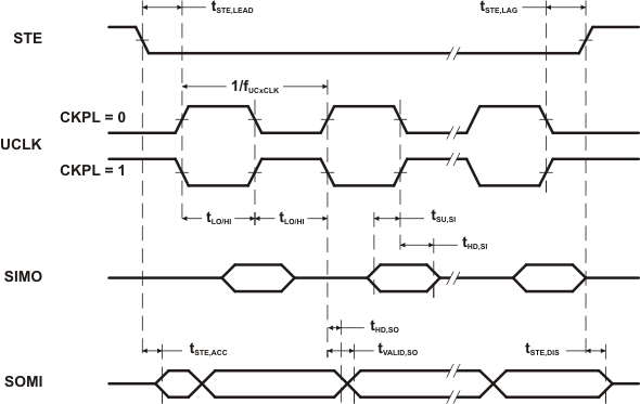 Figure 5-36 SPI Slave Mode, CKPH = 0
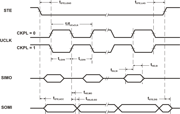 Figure 5-37 SPI Slave Mode, CKPH = 1
5.5.1.25 USCI (I2C Mode)
over recommended ranges of supply voltage and operating free-air temperature (unless otherwise noted) (see Figure 5-38)| PARAMETER | TEST CONDITIONS | VCC | MIN | TYP | MAX | UNIT | |
|---|---|---|---|---|---|---|---|
| fUSCI | USCI input clock frequency | SMCLK, duty cycle = 50% ± 10% | fSYSTEM | MHz | |||
| fSCL | SCL clock frequency | 3 V | 0 | 400 | kHz | ||
| tHD,STA | Hold time (repeated) START | fSCL ≤ 100 kHz | 3 V | 4.0 | µs | ||
| fSCL > 100 kHz | 0.6 | ||||||
| tSU,STA | Setup time for a repeated START | fSCL ≤ 100 kHz | 3 V | 4.7 | µs | ||
| fSCL > 100 kHz | 0.6 | ||||||
| tHD,DAT | Data hold time | 3 V | 0 | ns | |||
| tSU,DAT | Data setup time | 3 V | 250 | ns | |||
| tSU,STO | Setup time for STOP | 3 V | 4.0 | µs | |||
| tSP | Pulse width of spikes suppressed by input filter | 3 V | 50 | 100 | 600 | ns | |
 Figure 5-38 I2C Mode Timing
5.5.1.26 Comparator_A+
over recommended ranges of supply voltage and operating free-air temperature (unless otherwise noted)| PARAMETER | TEST CONDITIONS | VCC | MIN | TYP | MAX | UNIT | |
|---|---|---|---|---|---|---|---|
| I(DD)(1) | CAON = 1, CARSEL = 0, CAREF = 0 | 3 V | 45 | µA | |||
| I(Refladder/ RefDiode) | CAON = 1, CARSEL = 0, CAREF = 1/2/3, No load at CA0 and CA1 |
3 V | 45 | µA | |||
| V(IC) | Common–mode input voltage | CAON = 1 | 3 V | 0 | VCC-1 | V | |
| V(Ref025) | (Voltage at 0.25 VCC node) / VCC | PCA0 = 1, CARSEL = 1, CAREF = 1, No load at CA0 and CA1 |
3 V | 0.24 | |||
| V(Ref050) | (Voltage at 0.5 VCC node) / VCC | PCA0 = 1, CARSEL = 1, CAREF = 2, No load at CA0 and CA1 |
3 V | 0.48 | |||
| V(RefVT) | See Figure 5-39 and Figure 5-40 | PCA0 = 1, CARSEL = 1, CAREF = 3, No load at CA0 and CA1, TA = 85°C |
3 V | 490 | mV | ||
| V(offset) | Offset voltage(2) | 3 V | ±10 | mV | |||
| Vhys | Input hysteresis | CAON = 1 | 3 V | 0.7 | mV | ||
| t(response) | Response time (low-high and high-low) |
TA = 25°C, Overdrive 10 mV, Without filter: CAF = 0 |
3 V | 120 | ns | ||
| TA = 25°C, Overdrive 10 mV, With filter: CAF = 1 |
1.5 | µs | |||||
5.5.1.27 Typical Characteristics – Comparator_A+
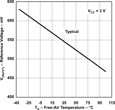 Figure 5-39 V(RefVT) vs Temperature, VCC = 3 V
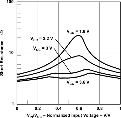 Figure 5-41 Short Resistance vs VIN/VCC
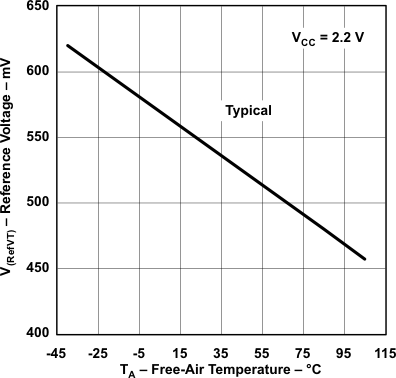 Figure 5-40 V(RefVT) vs Temperature, VCC = 2.2 V
5.5.1.28 10-Bit ADC, Power Supply and Input Range Conditions
over recommended ranges of supply voltage and operating free-air temperature (unless otherwise noted)(1)| PARAMETER | TEST CONDITIONS | TA | VCC | MIN | TYP | MAX | UNIT | |
|---|---|---|---|---|---|---|---|---|
| VCC | Analog supply voltage | VSS = 0 V | 2.2 | 3.6 | V | |||
| VAx | Analog input voltage(2) | All Ax terminals, Analog inputs selected in ADC10AE register | 3 V | 0 | VCC | V | ||
| IADC10 | ADC10 supply current(3) | fADC10CLK = 5.0 MHz, ADC10ON = 1, REFON = 0, ADC10SHT0 = 1, ADC10SHT1 = 0, ADC10DIV = 0 |
25°C | 3 V | 0.6 | mA | ||
| IREF+ | Reference supply current, reference buffer disabled(4) | fADC10CLK = 5.0 MHz, ADC10ON = 0, REF2_5V = 0, REFON = 1, REFOUT = 0 |
25°C | 3 V | 0.25 | mA | ||
| fADC10CLK = 5.0 MHz, ADC10ON = 0, REF2_5V = 1, REFON = 1, REFOUT = 0 |
0.25 | |||||||
| IREFB,0 | Reference buffer supply current with ADC10SR = 0(4) | fADC10CLK = 5.0 MHz, ADC10ON = 0, REFON = 1, REF2_5V = 0, REFOUT = 1, ADC10SR = 0 |
25°C | 3 V | 1.1 | mA | ||
| IREFB,1 | Reference buffer supply current with ADC10SR = 1(4) | fADC10CLK = 5.0 MHz, ADC10ON = 0, REFON = 1, REF2_5V = 0, REFOUT = 1, ADC10SR = 1 |
25°C | 3 V | 0.5 | mA | ||
| CI | Input capacitance | Only one terminal Ax can be selected at one time | 25°C | 3 V | 27 | pF | ||
| RI | Input MUX ON resistance | 0 V ≤ VAx ≤ VCC | 25°C | 3 V | 1000 | Ω | ||
- The leakage current is defined in the leakage current table with Px.y/Ax parameter.
- The analog input voltage range must be within the selected reference voltage range VR+ to VR– for valid conversion results.
- The internal reference supply current is not included in current consumption parameter IADC10.
- The internal reference current is supplied via terminal VCC. Consumption is independent of the ADC10ON control bit, unless a conversion is active. The REFON bit enables the built-in reference to settle before starting an A/D conversion.
5.5.1.29 10-Bit ADC, Built-In Voltage Reference
over recommended ranges of supply voltage and operating free-air temperature (unless otherwise noted)| PARAMETER | TEST CONDITIONS | VCC | MIN | TYP | MAX | UNIT | ||
|---|---|---|---|---|---|---|---|---|
| VCC,REF+ | Positive built-in reference analog supply voltage range | IVREF+ ≤ 1 mA, REF2_5V = 0 | 2.2 | V | ||||
| IVREF+ ≤ 1 mA, REF2_5V = 1 | 2.9 | |||||||
| VREF+ | Positive built-in reference voltage | IVREF+ ≤ IVREF+max, REF2_5V = 0 | 3 V | 1.41 | 1.5 | 1.59 | V | |
| IVREF+ ≤ IVREF+max, REF2_5V = 1 | 2.35 | 2.5 | 2.65 | |||||
| ILD,VREF+ | Maximum VREF+ load current | 3 V | ±1 | mA | ||||
| VREF+ load regulation | IVREF+ = 500 µA ± 100 µA, Analog input voltage VAx ≉ 0.75 V, REF2_5V = 0 |
3 V | ±2 | LSB | ||||
| IVREF+ = 500 µA ± 100 µA, Analog input voltage VAx ≉ 1.25 V, REF2_5V = 1 |
±2 | |||||||
| VREF+ load regulation response time | IVREF+ = 100 µA→900 µA, VAx ≉ 0.5 × VREF+, Error of conversion result ≤ 1 LSB, ADC10SR = 0 |
3 V | 400 | ns | ||||
| CVREF+ | Maximum capacitance at pin VREF+ | IVREF+ ≤ ±1 mA, REFON = 1, REFOUT = 1 | 3 V | 100 | pF | |||
| TCREF+ | Temperature coefficient | IVREF+ = const with 0 mA ≤ IVREF+ ≤ 1 mA | 3 V | ±100 | ppm/ °C | |||
| tREFON | Settling time of internal reference voltage to 99.9% VREF | IVREF+ = 0.5 mA, REF2_5V = 0, REFON = 0 → 1 |
3.6 V | 30 | µs | |||
| tREFBURST | Settling time of reference buffer to 99.9% VREF | IVREF+ = 0.5 mA, REF2_5V = 1, REFON = 1, REFBURST = 1, ADC10SR = 0 |
3 V | 2 | µs | |||
5.5.1.30 10-Bit ADC, External Reference
over recommended ranges of supply voltage and operating free-air temperature (unless otherwise noted)(1)| PARAMETER | TEST CONDITIONS | VCC | MIN | TYP | MAX | UNIT | |
|---|---|---|---|---|---|---|---|
| VEREF+ | Positive external reference input voltage range (2) | VEREF+ > VEREF–, SREF1 = 1, SREF0 = 0 |
1.4 | VCC | V | ||
| VEREF– ≤ VEREF+ ≤ VCC – 0.15 V, SREF1 = 1, SREF0 = 1 (3) |
1.4 | 3 | |||||
| VEREF– | Negative external reference input voltage range (4) | VEREF+ > VEREF– | 0 | 1.2 | V | ||
| ΔVEREF | Differential external reference input voltage range, ΔVEREF = VEREF+ – VEREF– |
VEREF+ > VEREF– (5) | 1.4 | VCC | V | ||
| IVEREF+ | Static input current into VEREF+ | 0 V ≤ VEREF+ ≤ VCC, SREF1 = 1, SREF0 = 0 |
3 V | ±1 | µA | ||
| 0 V ≤ VEREF+ ≤ VCC – 0.15 V ≤ 3 V, SREF1 = 1, SREF0 = 1(3) |
3 V | 0 | |||||
| IVEREF– | Static input current into VEREF– | 0 V ≤ VEREF– ≤ VCC | 3 V | ±1 | µA | ||
- The external reference is used during conversion to charge and discharge the capacitance array. The input capacitance, CI, is also the dynamic load for an external reference during conversion. The dynamic impedance of the reference supply should follow the recommendations on analog-source impedance to allow the charge to settle for 10-bit accuracy.
- The accuracy limits the minimum positive external reference voltage. Lower reference voltage levels may be applied with reduced accuracy requirements.
- Under this condition the external reference is internally buffered. The reference buffer is active and requires the reference buffer supply current IREFB. The current consumption can be limited to the sample and conversion period with REBURST = 1.
- The accuracy limits the maximum negative external reference voltage. Higher reference voltage levels may be applied with reduced accuracy requirements.
- The accuracy limits the minimum external differential reference voltage. Lower differential reference voltage levels may be applied with reduced accuracy requirements.
5.5.1.31 10-Bit ADC, Timing Parameters
over recommended ranges of supply voltage and operating free-air temperature (unless otherwise noted)| PARAMETER | TEST CONDITIONS | VCC | MIN | TYP | MAX | UNIT | ||
|---|---|---|---|---|---|---|---|---|
| fADC10CLK | ADC10 input clock frequency | For specified performance of ADC10 linearity parameters | ADC10SR = 0 | 3 V | 0.45 | 6.3 | MHz | |
| ADC10SR = 1 | 0.45 | 1.5 | ||||||
| fADC10OSC | ADC10 built-in oscillator frequency | ADC10DIVx = 0, ADC10SSELx = 0, fADC10CLK = fADC10OSC |
3 V | 3.7 | 6.3 | MHz | ||
| tCONVERT | Conversion time | ADC10 built-in oscillator, ADC10SSELx = 0, fADC10CLK = fADC10OSC |
3 V | 2.06 | 3.51 | µs | ||
| fADC10CLK from ACLK, MCLK, or SMCLK: ADC10SSELx ≠ 0 | 13 × ADC10DIV × 1/fADC10CLK |
|||||||
| tADC10ON | Turn-on settling time of the ADC | (1) | 100 | ns | ||||
5.5.1.32 10-Bit ADC, Linearity Parameters
over recommended ranges of supply voltage and operating free-air temperature (unless otherwise noted)| PARAMETER | TEST CONDITIONS | VCC | MIN | TYP | MAX | UNIT | |
|---|---|---|---|---|---|---|---|
| EI | Integral linearity error | 3 V | ±1 | LSB | |||
| ED | Differential linearity error | 3 V | ±1 | LSB | |||
| EO | Offset error | Source impedance RS < 100 Ω | 3 V | ±1 | LSB | ||
| EG | Gain error | 3 V | ±1.1 | ±2 | LSB | ||
| ET | Total unadjusted error | 3 V | ±2 | ±5 | LSB | ||
5.5.1.33 10-Bit ADC, Temperature Sensor and Built-In VMID
over recommended ranges of supply voltage and operating free-air temperature (unless otherwise noted)| PARAMETER | TEST CONDITIONS | VCC | MIN | TYP | MAX | UNIT | |
|---|---|---|---|---|---|---|---|
| ISENSOR | Temperature sensor supply current(1) | REFON = 0, INCHx = 0Ah, TA = 25°C |
3 V | 60 | µA | ||
| TCSENSOR | ADC10ON = 1, INCHx = 0Ah (2) | 3 V | 3.55 | mV/°C | |||
| tSensor(sample) | Sample time required if channel 10 is selected (3) | ADC10ON = 1, INCHx = 0Ah, Error of conversion result ≤ 1 LSB |
3 V | 30 | µs | ||
| IVMID | Current into divider at channel 11 | ADC10ON = 1, INCHx = 0Bh | 3 V | (4) | µA | ||
| VMID | VCC divider at channel 11 | ADC10ON = 1, INCHx = 0Bh, VMID ≉ 0.5 × VCC |
3 V | 1.5 | V | ||
| tVMID(sample) | Sample time required if channel 11 is selected (5) | ADC10ON = 1, INCHx = 0Bh, Error of conversion result ≤ 1 LSB |
3 V | 1220 | ns | ||
VSensor,typ = TCSensor (273 + T [°C] ) + VOffset,sensor [mV] or
VSensor,typ = TCSensor T [°C] + VSensor(TA = 0°C) [mV]
5.5.1.34 Flash Memory
over recommended ranges of supply voltage and operating free-air temperature (unless otherwise noted)| PARAMETER | TEST CONDITIONS | VCC | MIN | TYP | MAX | UNIT | |
|---|---|---|---|---|---|---|---|
| VCC(PGM/ERASE) | Program and erase supply voltage | 2.2 | 3.6 | V | |||
| fFTG | Flash timing generator frequency | 257 | 476 | kHz | |||
| IPGM | Supply current from VCC during program | 2.2 V/3.6 V | 1 | 5 | mA | ||
| IERASE | Supply current from VCC during erase | 2.2 V/3.6 V | 1 | 7 | mA | ||
| tCPT | Cumulative program time(1) | 2.2 V/3.6 V | 10 | ms | |||
| tCMErase | Cumulative mass erase time | 2.2 V/3.6 V | 20 | ms | |||
| Program/erase endurance | 104 | 105 | cycles | ||||
| tRetention | Data retention duration | TJ = 25°C | 100 | years | |||
| tWord | Word or byte program time | (2) | 30 | tFTG | |||
| tBlock, 0 | Block program time for first byte or word | (2) | 25 | tFTG | |||
| tBlock, 1-63 | Block program time for each additional byte or word | (2) | 18 | tFTG | |||
| tBlock, End | Block program end-sequence wait time | (2) | 6 | tFTG | |||
| tMass Erase | Mass erase time | (2) | 10593 | tFTG | |||
| tSeg Erase | Segment erase time | (2) | 4819 | tFTG | |||
5.5.1.35 RAM
over recommended ranges of supply voltage and operating free-air temperature (unless otherwise noted)| PARAMETER | TEST CONDITIONS | MIN | MAX | UNIT | |
|---|---|---|---|---|---|
| V(RAMh) | RAM retention supply voltage (1) | CPU halted | 1.6 | V | |
5.5.1.36 JTAG and Spy-Bi-Wire Interface
over recommended ranges of supply voltage and operating free-air temperature (unless otherwise noted)| PARAMETER | TEST CONDITIONS | VCC | MIN | TYP | MAX | UNIT | |
|---|---|---|---|---|---|---|---|
| fSBW | Spy-Bi-Wire input frequency | 2.2 V | 0 | 20 | MHz | ||
| tSBW,Low | Spy-Bi-Wire low clock pulse length | 2.2 V | 0.025 | 15 | µs | ||
| tSBW,En | Spy-Bi-Wire enable time (TEST high to acceptance of first clock edge(1)) |
2.2 V | 1 | µs | |||
| tSBW,Ret | Spy-Bi-Wire return to normal operation time | 2.2 V | 15 | 100 | µs | ||
| fTCK | TCK input frequency(2) | 2.2 V | 0 | 5 | MHz | ||
| RInternal | Internal pulldown resistance on TEST | 2.2 V | 25 | 60 | 90 | kΩ | |
5.5.1.37 JTAG Fuse
over recommended ranges of supply voltage and operating free-air temperature (unless otherwise noted)(1)| PARAMETER | TEST CONDITIONS | MIN | MAX | UNIT | |
|---|---|---|---|---|---|
| VCC(FB) | Supply voltage during fuse-blow condition | TA = 25°C | 2.5 | V | |
| VFB | Voltage level on TEST for fuse blow | 6 | 7 | V | |
| IFB | Supply current into TEST during fuse blow | 100 | mA | ||
| tFB | Time to blow fuse | 1 | ms | ||
5.5.2 MSP430 Core Operation
NOTE
For support and specific questions related to the MSP430 in the TPS65835 device, please refer to TI's E2E PMU forum and post relevant questions to the forum at the following link:
TI E2E PMU Forum.
- Title: TPS65835 "specific topic"
- Body: Question, with supporting code and oscilloscope screen captures if applicable.
Please format your posting as follows:
5.5.2.1 Description
The MSP430 integrated into the TPS65835 is from the MSP430x2xx family of ultralow-power microcontrollers. The architecture, combined with five low-power modes is optimized to achieve extended battery life in portable applications. The device features a powerful 16-bit RISC CPU, 16-bit registers, and constant generators that contribute to maximum code efficiency. The digitally controlled oscillator (DCO) allows wake-up from low-power modes to active mode in less than 1␣s. The list of the peripherals and modules included in this MSP430 are as follows:
- Up to 16 MHz CPU
- 16 kB Flash Memory
- 512 B RAM
- Basic Clock Module
- Internal Frequencies up to 16 MHz with one Calibrated Frequency
- Internal Very-Low-Power Low-Frequency (LF) Oscillator
- 32 kHz Crystal Support
- External Digital Clock Source
- 10-Bit ADC
- 200-ksps Analog-to-Digital (A/D) Converter with Internal Reference, Sample-and-Hold, and Autoscan
- Comparator A+ (Comp_A+)
- For Analog Signal Compare Function or Slope Analog-to-Digital (A/D) Conversion
- Timer0_A3 and Timer1_A3
- Up to Two 16-Bit Timer_A with Three Capture/Compare Registers
- Watchdog WDT+
- USCI A0, Universal Serial Communication Interface
- Enhanced UART Supporting Auto Baudrate Detection (LIN)
- IrDA Encoder and Decoder
- Synchronous SPI
- I2C
- USCI B0, Universal Serial Communication Interface
- Synchronous SPI
- I2C
- JTAG / Spy-By-Wire
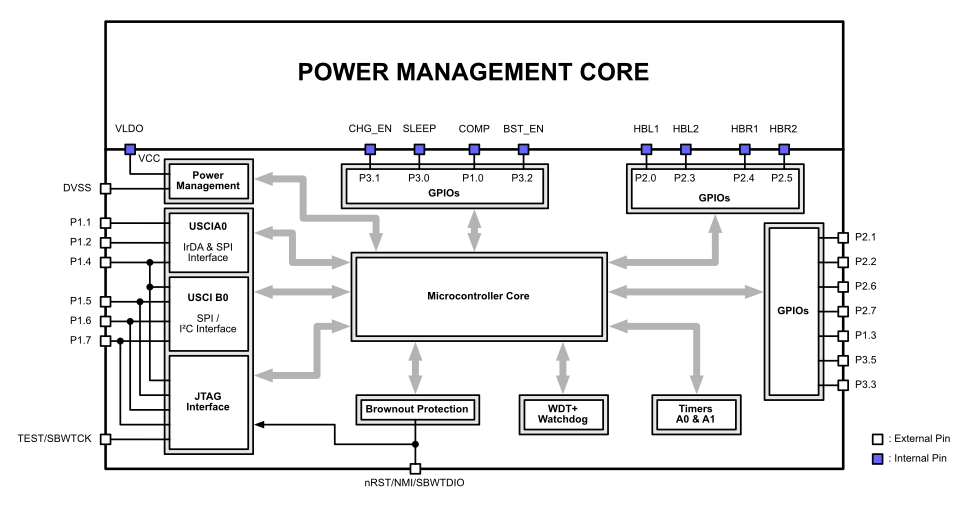 Figure 5-42 MSP430 Functional Block Diagram
5.5.2.2 Accessible MSP430 Pins
There are a number of internal pins connected between the MSP430 core and the power management core as well as external pins on the MSP430. Internal pins are not available externally but can be controlled by the MSP430 core in various ways. A table describing all available MSP430 pin functions (Table 5-7) along with a block diagram detailing the MSP430 core and the pin connectivity (see Figure 5-42) has been made available.
Table 5-7 Internally Connected Pins: MSP430 to Power Management Core
| POWER MANAGEMENT CORE PIN | MSP430 CORE PIN | FUNCTIONALITY | ||
|---|---|---|---|---|
| VLDO | AVCC / DVCC | Voltage supplied by LDO on power management core, connected to MSP430 power management module Enabled by SWITCH pin input |
||
| COMP | P1.0 / A0 / CA0 | Scaled down voltage of the BAT pin. Connected to Comparator_A+ channel CA0 or ADC channel A0 of the MSP430 To use COMP and Comp_A+ module function of the MSP430, the pin must be configured properly DO NOT CONFIGURE THIS PIN AS A GPIO AND PULL THIS PIN UP OR DOWN, THIS WILL INCREASE THE OPERATING CURRENT OF THE DEVICE |
||
| BST_EN | P3.2 | Enable pin for the boost on the power management core, ACTIVE HIGH | ||
| CHG_EN | P3.1 | Enable pin for the charger on the power management core, ACTIVE HIGH | ||
| SLEEP | P3.0 | Can put entire device into SLEEP state dependent upon system events, e.g., extended loss of IR or RF synchronization (1) | ||
| HBL1 | P2.0 | Control pin 1 for left frame of active shutter glasses | ||
| HBL2 | P2.3 | Control pin 2 for left frame of active shutter glasses | ||
| HBR1 | P2.4 | Control pin 1 for right frame of active shutter glasses | ||
| HBR2 | P2.5 | Control pin 2 for right frame of active shutter glasses | ||
Table 5-8 Externally Available MSP430 Pins
| PIN NAME | I/O | FUNCTIONALITY | ||
|---|---|---|---|---|
| P1.1/ TA0.0/ UCA0RXD/ UCA0SOMI/ A1/ CA1 |
I/O | General-purpose digital I/O pin Timer0_A, capture: CCI0A input, compare: Out0 output USCI_A0 receive data input in UART mode USCI_A0 slave data out/master in SPI mode ADC10 analog input A1 Comparator_A+, CA1 input |
||
| P1.2/ TA0.1/ UCA0TXD/ UCA0SIMO/ A2/ CA2 |
I/O | General-purpose digital I/O pin Timer0_A, capture: CCI1A input, compare: Out1 output USCI_A0 transmit data output in UART mode USCI_A0 slave data in/master out in SPI mode ADC10 analog input A2 Comparator_A+, CA2 input |
||
| P1.3/ ADC10CLK/ A3 VREF-/VEREF-/ CA3/ CAOUT |
I/O | General-purpose digital I/O pin ADC10, conversion clock output ADC10 analog input A3 ADC10 negative reference voltage Comparator_A+, CA3 input Comparator_A+, output |
||
| P1.4/ SMCLK/ UCB0STE UCA0CLK/ A4 VREF+/VEREF+/ CA4 TCK |
I/O | General-purpose digital I/O pin SMCLK signal output USCI_B0 slave transmit enable USCI_A0 clock input/output ADC10 analog input A4 ADC10 positive reference voltage Comparator_A+, CA4 input JTAG test clock, input terminal for device programming and test |
||
| P1.5/ TA0.0/ UCB0CLK/ UCA0STE/ A5/ CA5/ TMS |
I/O | General-purpose digital I/O pin Timer0_A, compare: Out0 output USCI_B0 clock input/output USCI_A0 slave transmit enable ADC10 analog input A5 Comparator_A+, CA5 input JTAG test mode select, input terminal for device programming and test |
||
| P1.6/ TA0.1/ A6/ CA6/ UCB0SOMI/ UCB0SCL/ TDI/TCLK |
I/O | General-purpose digital I/O pin Timer0_A, compare: Out1 output ADC10 analog input A6 Comparator_A+, CA6 input USCI_B0 slave out/master in SPI mode USCI_B0 SCL I2C clock in I2C mode JTAG test data input or test clock input during programming and test |
||
| P1.7/ A7/ CA7/ CAOUT/ UCB0SIMO/ UCB0SDA/ TDO/TDI |
I/O | General-purpose digital I/O pin ADC10 analog input A7 Comparator_A+, CA7 input Comparator_A+, output USCI_B0 slave in/master out in SPI mode USCI_B0 SDA I2C data in I2C mode JTAG test data output terminal or test data input during programming and test(1) |
||
| P2.1/ TA1.1 |
I/O | General-purpose digital I/O pin Timer1_A, capture: CCI1A input, compare: Out1 output |
||
| P2.2/ TA1.1 |
I/O | General-purpose digital I/O pin Timer1_A, capture: CCI1B input, compare: Out1 output |
||
| P2.6/ XIN/ TA0.1 |
I/O | General-purpose digital I/O pin XIN, Input terminal of crystal oscillator TA0.1, Timer0_A, compare: Out1 output |
||
| P2.7/ XOUT |
I/O | General-purpose digital I/O pin Output terminal of crystal oscillator(2)) |
||
| P3.3/ TA1.2 |
I/O | General-purpose digital I/O pin Timer1_A, compare: Out2 output |
||
| P3.5/ TA0.1 |
I/O | General-purpose digital I/O pin Timer0_A, compare: Out0 output |
||
| nRST/ NMI/ SBWTDIO |
I | Reset Nonmaskable interrupt input Spy-Bi-Wire test data input/output during programming and test |
||
| TEST/ SBWTCK |
I | Selects test mode for JTAG pins on Port 1. The device protection fuse is connected to TEST. Spy-Bi-Wire test clock input during programming and test |
||
| DVSS | N/A | MSP430 ground reference | ||
5.5.2.3 MSP430 Port Functions and Programming Options
This section details the programming options that are available for each of the pins that are accessible on the MSP430.
Table 5-9 Internal MSP430 Pin Functions and Programming Options
| PIN NAME (P_.x)(2) |
x | FUNCTION | MSP430 CONTROL BITS / SIGNALS (1) | ||||
|---|---|---|---|---|---|---|---|
| P_DIR.x | P_SEL.x | P_SEL2.x | ADC10AE.x
INCH.x=1 |
CAPD.y | |||
| P1.0/ | 0 | P1.x (I/O) | I: 0; O: 1 | 0 | 0 | 0 | 0 |
| A0/ | A0 | X | X | X | 1 (y = 0) | 0 | |
| CA0 | CA0 | X | X | X | 0 | 1 (y = 0) | |
| P2.0/ | 0 | P2.x (I/O), HBL1 internal signal | I: 0; O: 1 | 0 | 0 | — | — |
| TA1.0 | Timer1_A3.TA0 | 1 | 1 | 0 | — | — | |
| P2.3/ | 3 | P2.x (I/O), HBL2 internal signal | I: 0; O: 1 | 0 | 0 | — | — |
| TA1.0 | Timer1_A3.TA0 | 1 | 1 | 0 | — | — | |
| P2.4/ | 4 | P2.x (I/O), HBR1 internal signal | I: 0; O: 1 | 0 | 0 | — | — |
| TA1.2 | Timer1_A3.TA2 | 1 | 1 | 0 | — | — | |
| P2.5/ | 5 | P2.x (I/O), HBR2 internal signal | I: 0; O: 1 | 0 | 0 | — | — |
| TA1.2 | Timer1_A3.TA2 | 1 | 1 | 0 | — | — | |
| P3.0/ | 0 | P3.x (I/O), SLEEP signal | I: 0; O: 1 | 0 | 0 | — | — |
| TA0.2 | Timer0_A3.TA2 | 1 | 1 | 0 | — | — | |
| P3.1/ | 1 | P3.x (I/O), CHG_EN signal, ACTIVE HIGH | I: 0; O: 1 | 0 | 0 | — | — |
| TA1.2 | Timer1_A3.TA2 | 1 | 1 | 0 | — | — | |
| P3.2/ | 2 | P3.x (I/O), BST_EN signal, ACTIVE HIGH | I: 0; O: 1 | 0 | 0 | — | — |
| TA1.2 | Timer1_A3.TA2 | 1 | 1 | 0 | — | — | |
Table 5-10 External MSP430 Port 1 Functions and Programming Options
| PIN NAME (P1.x)(2) |
x | FUNCTION | MSP430 CONTROL BITS / SIGNALS (1) | ||||
|---|---|---|---|---|---|---|---|
| P1DIR.x | P1SEL.x | P1SEL2.x | ADC10AE.x
INCH.x=1 |
CAPD.y | |||
| P1.1/ | 1 | P1.x (I/O) | I: 0; O: 1 | 0 | 0 | 0 | 0 |
| TA0.0/ | TA0.0 | 1 | 1 | 0 | 0 | 0 | |
| TA0.CCI0A | 0 | 1 | 0 | 0 | 0 | ||
| UCA0RXD/ | UCA0RXD | from USCI | 1 | 1 | 0 | 0 | |
| UCA0SOMI/ | UCA0SOMI | from USCI | 1 | 1 | 0 | 0 | |
| A1/ | A1 | X | X | X | 1 (y = 1) | 0 | |
| CA1/ | CA1 | X | X | X | 0 | 1 (y = 1) | |
| Pin Osc | Capacitive sensing | X | 0 | 1 | 0 | 0 | |
| P1.2/ | 2 | P1.x (I/O) | I: 0; O: 1 | 0 | 0 | 0 | 0 |
| TA0.1/ | TA0.1 | 1 | 1 | 0 | 0 | 0 | |
| TA0.CCI1A | 0 | 1 | 0 | 0 | 0 | ||
| UCA0TXD/ | UCA0TXD | from USCI | 1 | 1 | 0 | 0 | |
| UCA0SIMO/ | UCA0SIMO | from USCI | 1 | 1 | 0 | 0 | |
| A2/ | A2 | X | X | X | 1 (y = 2) | 0 | |
| CA2/ | CA2 | X | X | X | 0 | 1 (y = 2) | |
| Pin Osc | Capacitive sensing | X | 0 | 1 | 0 | 0 | |
| P1.3/ | 3 | P1.x (I/O) | I: 0; O: 1 | 0 | 0 | 0 | 0 |
| ADC10CLK/ | ADC10CLK | 1 | 1 | 0 | 0 | 0 | |
| A3/ | A3 | X | X | X | 1 (y = 3) | 0 | |
| VREF-/ | VREF- | X | X | X | 1 | 0 | |
| VEREF-/ | VEREF- | X | X | X | 1 | 0 | |
| CA3 | CA3 | X | X | X | 0 | 1 (y = 3) | |
| Pin Osc | Capacitive sensing | X | 0 | 1 | 0 | 0 | |
| P1.4/ | 4 | P1.x (I/O) | I: 0; O: 1 | 0 | 0 | 0 | 0 |
| SMCLK/ | SMCLK | 1 | 1 | 0 | 0 | 0 | |
| UCB0STE/ | UCB0STE | from USCI | 1 | 1 | 1 (y = 4) | 0 | |
| UCA0CLK/ | UCA0CLK | from USCI | 1 | 1 | 1 (y = 4) | 0 | |
| VREF+/ | VREF+ | X | X | X | 1 | 0 | |
| VEREF+/ | VEREF+ | X | X | X | 1 | 0 | |
| A4/ | A4 | X | X | X | 1 (y = 4) | 0 | |
| CA4/ | CA4 | X | X | X | 0 | 1 (y = 4) | |
| TCK/ | TCK (JTAG Mode = 1) | X | X | X | 0 | 0 | |
| Pin Osc | Capacitive sensing | X | 0 | 1 | 0 | 0 | |
| P1.5/ | 5 | P1.x (I/O) | I: 0; O: 1 | 0 | 0 | 0 | 0 |
| TA0.0/ | TA0.0 | 1 | 1 | 0 | 0 | 0 | |
| UCB0CLK/ | UCB0CLK | from USCI | 1 | 1 | 0 | 0 | |
| UCA0STE/ | UCA0STE | from USCI | 1 | 1 | 0 | 0 | |
| A5/ | A5 | X | X | X | 1 (y = 5) | 0 | |
| CA5/ | CA5 | X | X | X | 0 | 1 (y = 5) | |
| TMS/ | TMS (JTAG Mode = 1) | X | X | X | 0 | 0 | |
| Pin Osc | Capacitive sensing | X | 0 | 1 | 0 | 0 | |
| P1.6/ | 6 | P1.x (I/O) | I: 0; O: 1 | 0 | 0 | 0 | 0 |
| TA0.1/ | TA0.1 | 1 | 1 | 0 | 0 | 0 | |
| UCB0SOMI/ | UCB0SOMI | from USCI | 1 | 1 | 0 | 0 | |
| UCB0SCL/ | UCB0SCL | from USCI | 1 | 1 | 0 | 0 | |
| A6/ | A6 | X | X | X | 1 (y = 6) | 0 | |
| CA6/ | CA6 | X | X | X | 0 | 1 (y = 6) | |
| TDI/TCLK/ | TDI/TCLK (JTAG Mode = 1) | X | X | X | 0 | 0 | |
| Pin Osc | Capacitive sensing | X | 0 | 1 | 0 | 0 | |
| P1.7/ | 7 | P1.x (I/O) | I: 0; O: 1 | 0 | 0 | 0 | 0 |
| UCB0SIMO/ | UCB0SIMO | from USCI | 1 | 1 | 0 | 0 | |
| UCB0SDA/ | UCB0SDA | from USCI | 1 | 1 | 0 | 0 | |
| A7/ | A7 | X | X | X | 1 (y = 7) | 0 | |
| CA7/ | CA7 | X | X | X | 0 | 1 (y = 7) | |
| CAOUT/ | CAOUT | 1 | 1 | 0 | 0 | 0 | |
| TDO/TDI/ | TDO/TDI (JTAG Mode = 1) | X | X | X | 0 | 0 | |
| Pin Osc | Capacitive sensing | X | 0 | 1 | 0 | 0 | |
Table 5-11 External MSP430 Port 2 Functions and Programming Options
| PIN NAME (P2.x)(2) |
x | FUNCTION | MSP430 CONTROL BITS / SIGNALS (1) | ||
|---|---|---|---|---|---|
| P2DIR.x | P2SEL.x | P2SEL2.x | |||
| P2.1/ | 1 | P2.x (I/O) | I: 0; O: 1 | 0 | 0 |
| TA1.1/ | Timer1_A3.CCI1A | 0 | 1 | 0 | |
| Timer1_A3.TA1 | 1 | 1 | 0 | ||
| Pin Osc | Capacitive sensing | X | 0 | 1 | |
| P2.2/ | 2 | P2.x (I/O) | I: 0; O: 1 | 0 | 0 |
| TA1.1/ | Timer1_A3.CCI1B | 0 | 1 | 0 | |
| Timer1_A3.TA1 | 1 | 1 | 0 | ||
| Pin Osc | Capacitive sensing | X | 0 | 1 | |
| P2.6/ | 6 | P2.x (I/O) | I: 0; O: 1 | 0 | 0 |
| XIN/ | XIN, LFXT1 Oscillator Input | 0 | 1 | 0 | |
| TA0.1/ | Timer0_A3.TA1 | 1 | 1 | 0 | |
| Pin Osc | Capacitive sensing | X | 0 | 1 | |
| P2.7/ | 7 | P2.x (I/O) | I: 0; O: 1 | 0 | 0 |
| XOUT/ | XOUT, LFXT1 Oscillator Output | 1 | 1 | 0 | |
| Pin Osc | Capacitive sensing | X | 0 | 1 | |
Table 5-12 External MSP430 Port 3 Functions and Programming Options
| PIN NAME (P3.x)(2) |
x | FUNCTION | MSP430 CONTROL BITS / SIGNALS (1) | ||
|---|---|---|---|---|---|
| P3DIR.x | P3SEL.x | P3SEL2.x | |||
| P3.3/ | 3 | P3.x (I/O) | I: 0; O: 1 | 0 | 0 |
| TA1.1/ | Timer1_A3.TA2 | 1 | 1 | 0 | |
| Pin Osc | Capacitive sensing | X | 0 | 1 | |
| P3.5/ | 5 | P3.x (I/O) | I: 0; O: 1 | 0 | 0 |
| TA1.1/ | Timer0_A3.TA2 | 1 | 1 | 0 | |
| Pin Osc | Capacitive sensing | X | 0 | 1 | |
5.5.2.4 Operating Modes
The MSP430 has one active mode and five software-selectable low-power modes of operation. An interrupt event can wake up the device from any of the five low-power modes, service the request, and restore back to the low-power mode on return from the interrupt program.
The following six operating modes can be configured by software:
- Active mode (AM)
- All clocks are active
- Low-power mode 0 (LPM0)
- CPU is disabled
- ACLK and SMCLK remain active, MCLK is disabled
- Low-power mode 1 (LPM1)
- CPU is disabled
- ACLK and SMCLK remain active, MCLK is disabled
- DCO's dc-generator is disabled if DCO not used in active mode
- Low-power mode 2 (LPM2)
- CPU is disabled
- MCLK and SMCLK are disabled
- DCO's dc-generator remains enabled
- ACLK remains active
- Low-power mode 3 (LPM3)
- CPU is disabled
- MCLK and SMCLK are disabled
- DCO's dc-generator is disabled
- ACLK remains active
- Low-power mode 4 (LPM4)
- CPU is disabled
- ACLK is disabled
- MCLK and SMCLK are disabled
- DCO's dc-generator is disabled
- Crystal oscillator is stopped
5.5.2.5 MSP430x2xx User's Guide
To view the user's guide for the MSP430 integrated into this device, see MSP430x2xx Family User's Guide. The list of peripherals found in this MSP430 is listed in the section: Section 5.5.2.1.