JAJSLW7B December 2020 – September 2023 TPS6593-Q1
PRODUCTION DATA
- 1
- 1 特長
- 2 アプリケーション
- 3 概要
- 4 Revision History
- 5 概要 (続き)
- 6 Pin Configuration and Functions
-
7 Specifications
- 7.1 Absolute Maximum Ratings
- 7.2 ESD Ratings
- 7.3 Recommended Operating Conditions
- 7.4 Thermal Information
- 7.5 General Purpose Low Drop-Out Regulators (LDO1, LDO2, LDO3)
- 7.6 Low Noise Low Drop-Out Regulator (LDO4)
- 7.7 Internal Low Drop-Out Regulators (LDOVRTC, LDOVINT)
- 7.8 BUCK1, BUCK2, BUCK3, BUCK4 and BUCK5 Regulators
- 7.9 Reference Generator (BandGap)
- 7.10 Monitoring Functions
- 7.11 Clocks, Oscillators, and PLL
- 7.12 Thermal Monitoring and Shutdown
- 7.13 System Control Thresholds
- 7.14 Current Consumption
- 7.15 Backup Battery Charger
- 7.16 Digital Input Signal Parameters
- 7.17 Digital Output Signal Parameters
- 7.18 I/O Pullup and Pulldown Resistance
- 7.19 I2C Interface
- 7.20 Serial Peripheral Interface (SPI)
- 7.21 Typical Characteristics
-
8 Detailed Description
- 8.1 Overview
- 8.2 Functional Block Diagram
- 8.3
Feature Description
- 8.3.1 System Supply Voltage Monitor
- 8.3.2
Power Resources (Bucks and LDOs)
- 8.3.2.1
Buck Regulators
- 8.3.2.1.1 BUCK Regulator Overview
- 8.3.2.1.2 Multi-Phase Operation and Phase-Adding or Shedding
- 8.3.2.1.3 Transition Between PWM and PFM Modes
- 8.3.2.1.4 Multi-Phase BUCK Regulator Configurations
- 8.3.2.1.5 Spread-Spectrum Mode
- 8.3.2.1.6 Adaptive Voltage Scaling (AVS) and Dynamic Voltage Scaling (DVS) Support
- 8.3.2.1.7 BUCK Output Voltage Setting
- 8.3.2.1.8 BUCK Regulator Current Limit
- 8.3.2.1.9 SW_Bx Short-to-Ground Detection
- 8.3.2.1.10 Sync Clock Functionality
- 49
- 8.3.2.2 Low Dropout Regulators (LDOs)
- 8.3.2.1
Buck Regulators
- 8.3.3 Output Voltage Monitor and PGOOD Generation
- 8.3.4 Thermal Monitoring
- 8.3.5 Backup Supply Power-Path
- 8.3.6 General-Purpose I/Os (GPIO Pins)
- 8.3.7 nINT, EN_DRV, and nRSTOUT Pins
- 8.3.8 Interrupts
- 8.3.9 RTC
- 8.3.10
Watchdog (WDOG)
- 8.3.10.1 Watchdog Fail Counter and Status
- 8.3.10.2 Watchdog Start-Up and Configuration
- 8.3.10.3 MCU to Watchdog Synchronization
- 8.3.10.4 Watchdog Disable Function
- 8.3.10.5 Watchdog Sequence
- 8.3.10.6 Watchdog Trigger Mode
- 8.3.10.7 WatchDog Flow Chart and Timing Diagrams in Trigger Mode
- 79
- 8.3.10.8 Watchdog Question-Answer Mode
- 8.3.11 Error Signal Monitor (ESM)
- 8.4
Device Functional Modes
- 8.4.1
Device State Machine
- 8.4.1.1 Fixed Device Power FSM
- 8.4.1.2
Pre-Configurable Mission States
- 8.4.1.2.1
PFSM Commands
- 8.4.1.2.1.1 REG_WRITE_IMM Command
- 8.4.1.2.1.2 REG_WRITE_MASK_IMM Command
- 8.4.1.2.1.3 REG_WRITE_MASK_PAGE0_IMM Command
- 8.4.1.2.1.4 REG_WRITE_BIT_PAGE0_IMM Command
- 8.4.1.2.1.5 REG_WRITE_WIN_PAGE0_IMM Command
- 8.4.1.2.1.6 REG_WRITE_VOUT_IMM Command
- 8.4.1.2.1.7 REG_WRITE_VCTRL_IMM Command
- 8.4.1.2.1.8 REG_WRITE_MASK_SREG Command
- 8.4.1.2.1.9 SREG_READ_REG Command
- 8.4.1.2.1.10 SREG_WRITE_IMM Command
- 8.4.1.2.1.11 WAIT Command
- 8.4.1.2.1.12 DELAY_IMM Command
- 8.4.1.2.1.13 DELAY_SREG Command
- 8.4.1.2.1.14 TRIG_SET Command
- 8.4.1.2.1.15 TRIG_MASK Command
- 8.4.1.2.1.16 END Command
- 8.4.1.2.2 Configuration Memory Organization and Sequence Execution
- 8.4.1.2.3 Mission State Configuration
- 8.4.1.2.4 Pre-Configured Hardware Transitions
- 8.4.1.2.1
PFSM Commands
- 8.4.1.3 Error Handling Operations
- 8.4.1.4 Device Start-up Timing
- 8.4.1.5 Power Sequences
- 8.4.1.6 First Supply Detection
- 8.4.1.7 Register Power Domains and Reset Levels
- 8.4.2 Multi-PMIC Synchronization
- 8.4.1
Device State Machine
- 8.5 Control Interfaces
- 8.6 Configurable Registers
- 8.7 Register Maps
- 9 Application and Implementation
- 10Device and Documentation Support
- 11Mechanical, Packaging, and Orderable Information
パッケージ・オプション
メカニカル・データ(パッケージ|ピン)
- RWE|56
サーマルパッド・メカニカル・データ
- RWE|56
発注情報
9.4.2 Layout Example
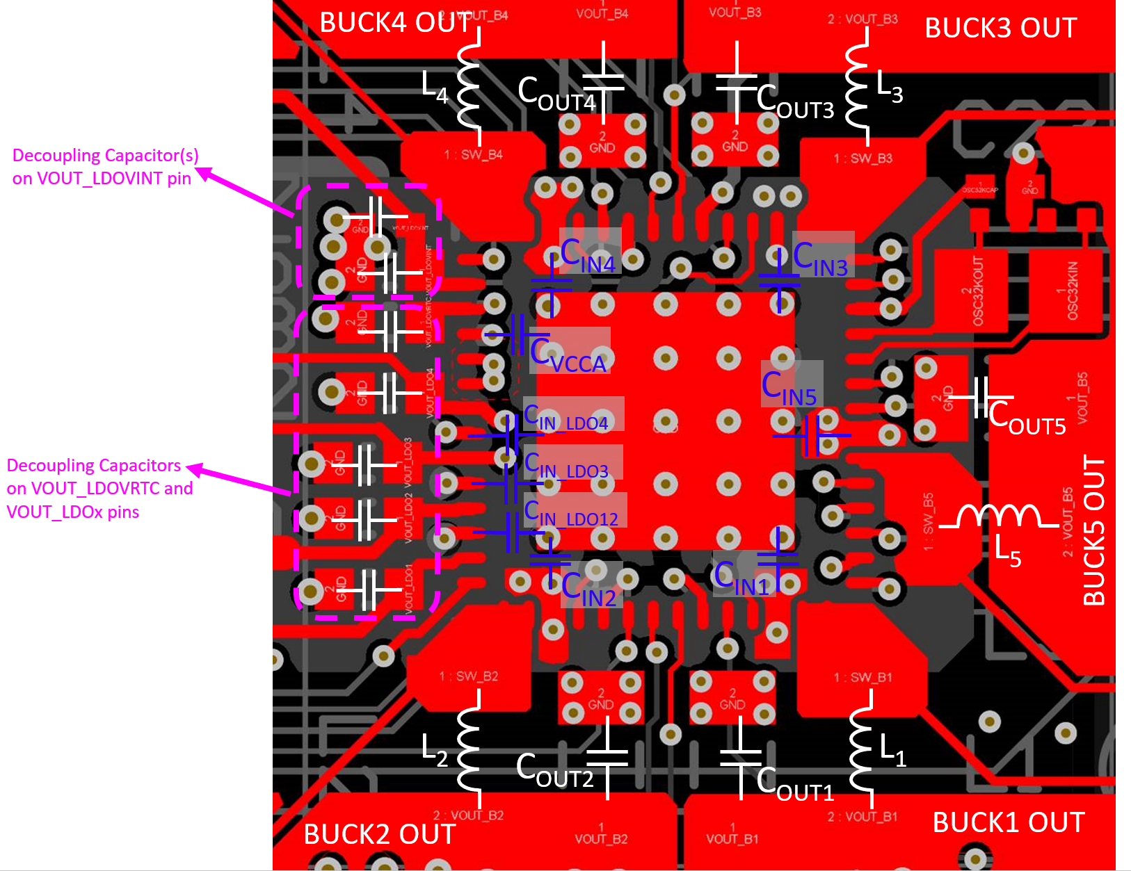
 Figure 9-70 Example
PMIC Layout
Figure 9-70 Example
PMIC LayoutThis example shows a top and bottom layout of the key power components and the crystal oscillator based on the EVM. Most of the digital routing is neglected in this image, see the EVM design files EVM design files for full details. The highest priority must be on the buck input capacitors, followed by the inductors, and the output capacitor on the VOUT_LDOVINT pin. Ensure that there are sufficient vias for high current pathways.