JAJSLW7B December 2020 – September 2023 TPS6593-Q1
PRODUCTION DATA
- 1
- 1 特長
- 2 アプリケーション
- 3 概要
- 4 Revision History
- 5 概要 (続き)
- 6 Pin Configuration and Functions
-
7 Specifications
- 7.1 Absolute Maximum Ratings
- 7.2 ESD Ratings
- 7.3 Recommended Operating Conditions
- 7.4 Thermal Information
- 7.5 General Purpose Low Drop-Out Regulators (LDO1, LDO2, LDO3)
- 7.6 Low Noise Low Drop-Out Regulator (LDO4)
- 7.7 Internal Low Drop-Out Regulators (LDOVRTC, LDOVINT)
- 7.8 BUCK1, BUCK2, BUCK3, BUCK4 and BUCK5 Regulators
- 7.9 Reference Generator (BandGap)
- 7.10 Monitoring Functions
- 7.11 Clocks, Oscillators, and PLL
- 7.12 Thermal Monitoring and Shutdown
- 7.13 System Control Thresholds
- 7.14 Current Consumption
- 7.15 Backup Battery Charger
- 7.16 Digital Input Signal Parameters
- 7.17 Digital Output Signal Parameters
- 7.18 I/O Pullup and Pulldown Resistance
- 7.19 I2C Interface
- 7.20 Serial Peripheral Interface (SPI)
- 7.21 Typical Characteristics
-
8 Detailed Description
- 8.1 Overview
- 8.2 Functional Block Diagram
- 8.3
Feature Description
- 8.3.1 System Supply Voltage Monitor
- 8.3.2
Power Resources (Bucks and LDOs)
- 8.3.2.1
Buck Regulators
- 8.3.2.1.1 BUCK Regulator Overview
- 8.3.2.1.2 Multi-Phase Operation and Phase-Adding or Shedding
- 8.3.2.1.3 Transition Between PWM and PFM Modes
- 8.3.2.1.4 Multi-Phase BUCK Regulator Configurations
- 8.3.2.1.5 Spread-Spectrum Mode
- 8.3.2.1.6 Adaptive Voltage Scaling (AVS) and Dynamic Voltage Scaling (DVS) Support
- 8.3.2.1.7 BUCK Output Voltage Setting
- 8.3.2.1.8 BUCK Regulator Current Limit
- 8.3.2.1.9 SW_Bx Short-to-Ground Detection
- 8.3.2.1.10 Sync Clock Functionality
- 49
- 8.3.2.2 Low Dropout Regulators (LDOs)
- 8.3.2.1
Buck Regulators
- 8.3.3 Output Voltage Monitor and PGOOD Generation
- 8.3.4 Thermal Monitoring
- 8.3.5 Backup Supply Power-Path
- 8.3.6 General-Purpose I/Os (GPIO Pins)
- 8.3.7 nINT, EN_DRV, and nRSTOUT Pins
- 8.3.8 Interrupts
- 8.3.9 RTC
- 8.3.10
Watchdog (WDOG)
- 8.3.10.1 Watchdog Fail Counter and Status
- 8.3.10.2 Watchdog Start-Up and Configuration
- 8.3.10.3 MCU to Watchdog Synchronization
- 8.3.10.4 Watchdog Disable Function
- 8.3.10.5 Watchdog Sequence
- 8.3.10.6 Watchdog Trigger Mode
- 8.3.10.7 WatchDog Flow Chart and Timing Diagrams in Trigger Mode
- 79
- 8.3.10.8 Watchdog Question-Answer Mode
- 8.3.11 Error Signal Monitor (ESM)
- 8.4
Device Functional Modes
- 8.4.1
Device State Machine
- 8.4.1.1 Fixed Device Power FSM
- 8.4.1.2
Pre-Configurable Mission States
- 8.4.1.2.1
PFSM Commands
- 8.4.1.2.1.1 REG_WRITE_IMM Command
- 8.4.1.2.1.2 REG_WRITE_MASK_IMM Command
- 8.4.1.2.1.3 REG_WRITE_MASK_PAGE0_IMM Command
- 8.4.1.2.1.4 REG_WRITE_BIT_PAGE0_IMM Command
- 8.4.1.2.1.5 REG_WRITE_WIN_PAGE0_IMM Command
- 8.4.1.2.1.6 REG_WRITE_VOUT_IMM Command
- 8.4.1.2.1.7 REG_WRITE_VCTRL_IMM Command
- 8.4.1.2.1.8 REG_WRITE_MASK_SREG Command
- 8.4.1.2.1.9 SREG_READ_REG Command
- 8.4.1.2.1.10 SREG_WRITE_IMM Command
- 8.4.1.2.1.11 WAIT Command
- 8.4.1.2.1.12 DELAY_IMM Command
- 8.4.1.2.1.13 DELAY_SREG Command
- 8.4.1.2.1.14 TRIG_SET Command
- 8.4.1.2.1.15 TRIG_MASK Command
- 8.4.1.2.1.16 END Command
- 8.4.1.2.2 Configuration Memory Organization and Sequence Execution
- 8.4.1.2.3 Mission State Configuration
- 8.4.1.2.4 Pre-Configured Hardware Transitions
- 8.4.1.2.1
PFSM Commands
- 8.4.1.3 Error Handling Operations
- 8.4.1.4 Device Start-up Timing
- 8.4.1.5 Power Sequences
- 8.4.1.6 First Supply Detection
- 8.4.1.7 Register Power Domains and Reset Levels
- 8.4.2 Multi-PMIC Synchronization
- 8.4.1
Device State Machine
- 8.5 Control Interfaces
- 8.6 Configurable Registers
- 8.7 Register Maps
- 9 Application and Implementation
- 10Device and Documentation Support
- 11Mechanical, Packaging, and Orderable Information
パッケージ・オプション
メカニカル・データ(パッケージ|ピン)
- RWE|56
サーマルパッド・メカニカル・データ
- RWE|56
発注情報
8.4.1.5 Power Sequences
A power sequence is an automatic preconfigured sequence the TPS6593-Q1 device applies to its resources, which include the states of the BUCKs, LDOs, 32-kHz clock and the GPIO output signals. For a detailed description of the GPIOs signals, please refer to General-Purpose I/Os (GPIO Pins).
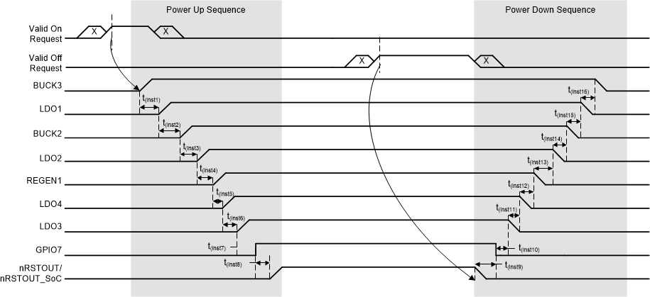
Figure 8-42 shows an example of a power up transition followed by a power down transition. The power up sequence is triggered through a valid on request, and the power down sequence is trigger by a valid off request. The resources controlled (for this example) are: BUCK3, LDO1, BUCK2, LDO2, GPIO1, LDO4, and LDO3. The time between each resource enable and disable (TinstX) is also part of the preconfigured sequence definition.
A resource not assigned to any power sequence remains in off mode during the power-up sequence. The attached MCU or SoC can enable and configure this resource independently when the power-up sequence completes. Also the EN_DRV remains low during the power-up sequence. The attached MCU or SoC can release the EN_DRV pin by setting the ENABLE_DRV bit (requires running watchdog, ESM started and no pending interrupt bits).
 Figure 8-42 Power Sequence
Example
Figure 8-42 Power Sequence
ExampleAs the power sequences of the TPS6593-Q1 device are defined according to the processor requirements, the total time for the completion of the power sequence varies across various system definitions.