JAJSIA2B December 2019 – February 2022 TPS6594-Q1
PRODUCTION DATA
- 1 特長
- 2 アプリケーション
- 3 概要
- 4 Revision History
- 5 概要 (続き)
- 6 Pin Configuration and Functions
-
7 Specifications
- 7.1 Absolute Maximum Ratings
- 7.2 ESD Ratings
- 7.3 Recommended Operating Conditions
- 7.4 Thermal Information
- 7.5 General Purpose Low Drop-Out Regulators (LDO1, LDO2, LDO3)
- 7.6 Low Noise Low Drop-Out Regulator (LDO4)
- 7.7 Internal Low Drop-Out Regulators (LDOVRTC, LDOVINT)
- 7.8 BUCK1, BUCK2, BUCK3, BUCK4 and BUCK5 Regulators
- 7.9 Reference Generator (BandGap)
- 7.10 Monitoring Functions
- 7.11 Clocks, Oscillators, and PLL
- 7.12 Thermal Monitoring and Shutdown
- 7.13 System Control Thresholds
- 7.14 Current Consumption
- 7.15 Backup Battery Charger
- 7.16 Digital Input Signal Parameters
- 7.17 Digital Output Signal Parameters
- 7.18 I/O Pullup and Pulldown Resistance
- 7.19 I2C Interface
- 7.20 Serial Peripheral Interface (SPI)
- 7.21 Typical Characteristics
-
8 Detailed Description
- 8.1 Overview
- 8.2 Functional Block Diagram
- 8.3
Feature Description
- 8.3.1 System Supply Voltage Monitor and Over-Voltage Protection
- 8.3.2
Power Resources (Bucks and LDOs)
- 8.3.2.1
Buck Regulators
- 8.3.2.1.1 BUCK Regulator Overview
- 8.3.2.1.2 Multi-Phase Operation and Phase-Adding or Shedding
- 8.3.2.1.3 Transition Between PWM and PFM Modes
- 8.3.2.1.4 Multi-Phase BUCK Regulator Configurations
- 8.3.2.1.5 Spread-Spectrum Mode
- 8.3.2.1.6 Adaptive Voltage Scaling (AVS) and Dynamic Voltage Scaling (DVS) Support
- 8.3.2.1.7 BUCK Output Voltage Setting
- 8.3.2.1.8 BUCK Regulator Current Limit
- 8.3.2.1.9 SW_Bx Short-to-Ground Detection
- 8.3.2.1.10 Sync Clock Functionality
- 48
- 8.3.2.2 Low Dropout Regulators (LDOs)
- 8.3.2.1
Buck Regulators
- 8.3.3 Residual Voltage Checking
- 8.3.4 Output Voltage Monitor and PGOOD Generation
- 8.3.5 Thermal Monitoring
- 8.3.6 Backup Supply Power-Path
- 8.3.7 General-Purpose I/Os (GPIO Pins)
- 8.3.8 nINT, EN_DRV, and nRSTOUT Pins
- 8.3.9 Interrupts
- 8.3.10 RTC
- 8.3.11
Watchdog (WDOG)
- 8.3.11.1 Watchdog Fail Counter and Status
- 8.3.11.2 Watchdog Start-Up and Configuration
- 8.3.11.3 MCU to Watchdog Synchronization
- 8.3.11.4 Watchdog Disable Function
- 8.3.11.5 Watchdog Sequence
- 8.3.11.6 Watchdog Trigger Mode
- 8.3.11.7 WatchDog Flow Chart and Timing Diagrams in Trigger Mode
- 79
- 8.3.11.8 Watchdog Question-Answer Mode
- 8.3.12 Error Signal Monitor (ESM)
- 8.4
Device Functional Modes
- 8.4.1
Device State Machine
- 8.4.1.1 Fixed Device Power FSM
- 8.4.1.2
Pre-Configurable Mission States
- 8.4.1.2.1
PFSM Commands
- 8.4.1.2.1.1 REG_WRITE_IMM Command
- 8.4.1.2.1.2 REG_WRITE_MASK_IMM Command
- 8.4.1.2.1.3 REG_WRITE_MASK_PAGE0_IMM Command
- 8.4.1.2.1.4 REG_WRITE_BIT_PAGE0_IMM Command
- 8.4.1.2.1.5 REG_WRITE_WIN_PAGE0_IMM Command
- 8.4.1.2.1.6 REG_WRITE_VOUT_IMM Command
- 8.4.1.2.1.7 REG_WRITE_VCTRL_IMM Command
- 8.4.1.2.1.8 REG_WRITE_MASK_SREG Command
- 8.4.1.2.1.9 SREG_READ_REG Command
- 8.4.1.2.1.10 SREG_WRITE_IMM Command
- 8.4.1.2.1.11 WAIT Command
- 8.4.1.2.1.12 DELAY_IMM Command
- 8.4.1.2.1.13 DELAY_SREG Command
- 8.4.1.2.1.14 TRIG_SET Command
- 8.4.1.2.1.15 TRIG_MASK Command
- 8.4.1.2.1.16 END Command
- 8.4.1.2.2 Configuration Memory Organization and Sequence Execution
- 8.4.1.2.3 Mission State Configuration
- 8.4.1.2.4 Pre-Configured Hardware Transitions
- 8.4.1.2.1
PFSM Commands
- 8.4.1.3 Error Handling Operations
- 8.4.1.4 Device Start-up Timing
- 8.4.1.5 Power Sequences
- 8.4.1.6 First Supply Detection
- 8.4.1.7 Register Power Domains and Reset Levels
- 8.4.2 Multi-PMIC Synchronization
- 8.4.1
Device State Machine
- 8.5 Control Interfaces
- 8.6 Configurable Registers
- 8.7 Register Maps
- 9 Application and Implementation
- 10Power Supply Recommendations
- 11Layout
- 12Device and Documentation Support
- 13Mechanical, Packaging, and Orderable Information
パッケージ・オプション
メカニカル・データ(パッケージ|ピン)
- RWE|56
サーマルパッド・メカニカル・データ
- RWE|56
発注情報
8.4.1.2.4.5 LP_WKUP Pins for Waking Up from LP STANDBY
The LP_WKUP functions are activated through the edge detection of LP_WKUP pins, configurable as secondary functions of GPIO3 and GPIO4. They are specially designed to wake the device up from the LP STANDBY state when a high speed wake-up signal is detected. Similar to the WKUP1 and WKUP2 pins, when GPIO3 or GPIO4 pin is configured as an LP_WKUP1 pin, a rising or falling edge detected at the input of this pin (configurable by the GPIOn_FALL_MASK and the GPIOn_RISE_MASK bits) wakes up the device to the ACTIVE state. Likewise, if the pin is configured as an LP_WKUP2 pin, a detected edge wakes up the device to the MCU ONLY state. If multiple edge detections of LP_WKUP signals occur simultaneously, the device goes to the state in the following priority order:
- ACTIVE
- MCU ONLY
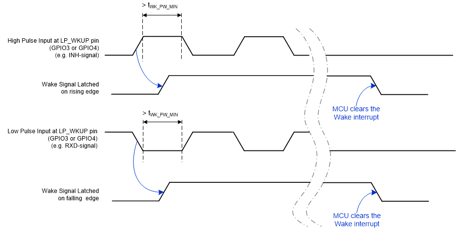
The TPS6594-Q1 device supports limited CAN wake-up capability through the LP_WKUP1/2 pins. When an input signal (without deglitch) with logic level transition from high-to-low or low-to-high with a minimum pulse width of tWK_PW_MIN is detected on the assigned LP_WKUP1/2 pins, the device wakes up asynchronously and executes the power up sequence. CAN-transceiver RXD- or INH-outputs can be connected to the LP_WKUP pin. If RXD-output is used, it is assumed that the transceiver RXD-pin IO is powered by the transceiver itself from an external supply when TPS6594-Q1 is in the LP_STANDBY state. If INH-signal is used it has to be scaled down to the recommenced GPIO input voltage level specified in the electrical characteristics table.
In this PFSM example, the device can wake up from the LP_STANDBY state through the detection of LP_WKUP pins only if it enters the LP_STANDBY state through the TRIGGER_I2C_0 OFF request while the NSLEEPn signals are masked, and the on request initialized by the nPWRON/ENABLE pin remains active. Once a valid wake-up signal is detected at the LP_WKUP pin, it is handled as a WAKE request. The nINT pin generates an interrupt to signal the MCU of the wake-up event, and the corresponding GPIOx_INT interrupt bit is set. The wake request remains active until the interrupt bit is cleared by the MCU. Table 8-20 shows how the device returns to the state indicated by the NSLEEP1 and NSLEEP2 signals after the wake request is canceled.
Figure 8-43 illustrates the valid wake-up signal at the LP_WKUP1/2 pins, and the generation and clearing of the internal wake-up signal.
 Figure 8-43 CAN Wake-Up Timing
Diagram