JAJSIA2B December 2019 – February 2022 TPS6594-Q1
PRODUCTION DATA
- 1 特長
- 2 アプリケーション
- 3 概要
- 4 Revision History
- 5 概要 (続き)
- 6 Pin Configuration and Functions
-
7 Specifications
- 7.1 Absolute Maximum Ratings
- 7.2 ESD Ratings
- 7.3 Recommended Operating Conditions
- 7.4 Thermal Information
- 7.5 General Purpose Low Drop-Out Regulators (LDO1, LDO2, LDO3)
- 7.6 Low Noise Low Drop-Out Regulator (LDO4)
- 7.7 Internal Low Drop-Out Regulators (LDOVRTC, LDOVINT)
- 7.8 BUCK1, BUCK2, BUCK3, BUCK4 and BUCK5 Regulators
- 7.9 Reference Generator (BandGap)
- 7.10 Monitoring Functions
- 7.11 Clocks, Oscillators, and PLL
- 7.12 Thermal Monitoring and Shutdown
- 7.13 System Control Thresholds
- 7.14 Current Consumption
- 7.15 Backup Battery Charger
- 7.16 Digital Input Signal Parameters
- 7.17 Digital Output Signal Parameters
- 7.18 I/O Pullup and Pulldown Resistance
- 7.19 I2C Interface
- 7.20 Serial Peripheral Interface (SPI)
- 7.21 Typical Characteristics
-
8 Detailed Description
- 8.1 Overview
- 8.2 Functional Block Diagram
- 8.3
Feature Description
- 8.3.1 System Supply Voltage Monitor and Over-Voltage Protection
- 8.3.2
Power Resources (Bucks and LDOs)
- 8.3.2.1
Buck Regulators
- 8.3.2.1.1 BUCK Regulator Overview
- 8.3.2.1.2 Multi-Phase Operation and Phase-Adding or Shedding
- 8.3.2.1.3 Transition Between PWM and PFM Modes
- 8.3.2.1.4 Multi-Phase BUCK Regulator Configurations
- 8.3.2.1.5 Spread-Spectrum Mode
- 8.3.2.1.6 Adaptive Voltage Scaling (AVS) and Dynamic Voltage Scaling (DVS) Support
- 8.3.2.1.7 BUCK Output Voltage Setting
- 8.3.2.1.8 BUCK Regulator Current Limit
- 8.3.2.1.9 SW_Bx Short-to-Ground Detection
- 8.3.2.1.10 Sync Clock Functionality
- 48
- 8.3.2.2 Low Dropout Regulators (LDOs)
- 8.3.2.1
Buck Regulators
- 8.3.3 Residual Voltage Checking
- 8.3.4 Output Voltage Monitor and PGOOD Generation
- 8.3.5 Thermal Monitoring
- 8.3.6 Backup Supply Power-Path
- 8.3.7 General-Purpose I/Os (GPIO Pins)
- 8.3.8 nINT, EN_DRV, and nRSTOUT Pins
- 8.3.9 Interrupts
- 8.3.10 RTC
- 8.3.11
Watchdog (WDOG)
- 8.3.11.1 Watchdog Fail Counter and Status
- 8.3.11.2 Watchdog Start-Up and Configuration
- 8.3.11.3 MCU to Watchdog Synchronization
- 8.3.11.4 Watchdog Disable Function
- 8.3.11.5 Watchdog Sequence
- 8.3.11.6 Watchdog Trigger Mode
- 8.3.11.7 WatchDog Flow Chart and Timing Diagrams in Trigger Mode
- 79
- 8.3.11.8 Watchdog Question-Answer Mode
- 8.3.12 Error Signal Monitor (ESM)
- 8.4
Device Functional Modes
- 8.4.1
Device State Machine
- 8.4.1.1 Fixed Device Power FSM
- 8.4.1.2
Pre-Configurable Mission States
- 8.4.1.2.1
PFSM Commands
- 8.4.1.2.1.1 REG_WRITE_IMM Command
- 8.4.1.2.1.2 REG_WRITE_MASK_IMM Command
- 8.4.1.2.1.3 REG_WRITE_MASK_PAGE0_IMM Command
- 8.4.1.2.1.4 REG_WRITE_BIT_PAGE0_IMM Command
- 8.4.1.2.1.5 REG_WRITE_WIN_PAGE0_IMM Command
- 8.4.1.2.1.6 REG_WRITE_VOUT_IMM Command
- 8.4.1.2.1.7 REG_WRITE_VCTRL_IMM Command
- 8.4.1.2.1.8 REG_WRITE_MASK_SREG Command
- 8.4.1.2.1.9 SREG_READ_REG Command
- 8.4.1.2.1.10 SREG_WRITE_IMM Command
- 8.4.1.2.1.11 WAIT Command
- 8.4.1.2.1.12 DELAY_IMM Command
- 8.4.1.2.1.13 DELAY_SREG Command
- 8.4.1.2.1.14 TRIG_SET Command
- 8.4.1.2.1.15 TRIG_MASK Command
- 8.4.1.2.1.16 END Command
- 8.4.1.2.2 Configuration Memory Organization and Sequence Execution
- 8.4.1.2.3 Mission State Configuration
- 8.4.1.2.4 Pre-Configured Hardware Transitions
- 8.4.1.2.1
PFSM Commands
- 8.4.1.3 Error Handling Operations
- 8.4.1.4 Device Start-up Timing
- 8.4.1.5 Power Sequences
- 8.4.1.6 First Supply Detection
- 8.4.1.7 Register Power Domains and Reset Levels
- 8.4.2 Multi-PMIC Synchronization
- 8.4.1
Device State Machine
- 8.5 Control Interfaces
- 8.6 Configurable Registers
- 8.7 Register Maps
- 9 Application and Implementation
- 10Power Supply Recommendations
- 11Layout
- 12Device and Documentation Support
- 13Mechanical, Packaging, and Orderable Information
パッケージ・オプション
メカニカル・データ(パッケージ|ピン)
- RWE|56
サーマルパッド・メカニカル・データ
- RWE|56
発注情報
9.2.1.2.3 Crystal Oscillator
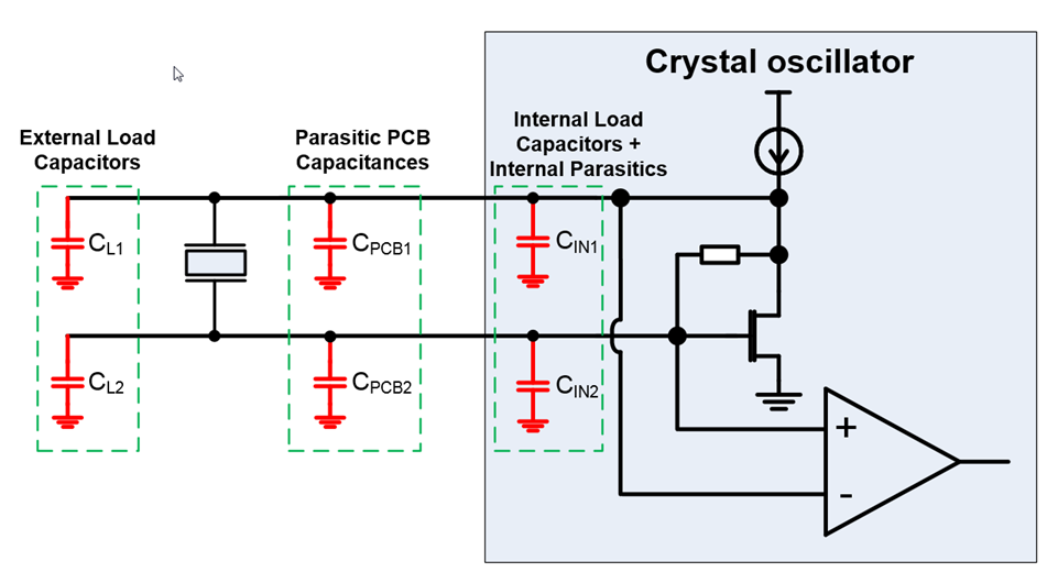
A crystal oscillator can be used for application requiring a high accuracy real-time clock module. The OSC32KCAP pin is bypassed with a 100-nF bypass capacitor for noise rejection. For the OSC32KIN and OSC32KOUT pins, a simplified oscillator schematic is shown in Figure 9-2 to determine what external load capacitors are needed for the crystal.
 Figure 9-2 Crystal Oscillator Component Selection
CIN1 and CIN2 are both 12-pF for this device. CPCB1 and CPCB2 depend on the board but is generally around 1-pF. The crystal oscillator chosen must have a required load capacitance of either 6-pF, 9-pF, or 12.5-pF and the value of the XTAL_SEL bit in the RTC_CTRL_2 register must be updated based on the oscillator chosen. To achieve the required load capacitance (CL) for the oscillator, Equation 26 is used. It assumes that the crystal series capacitance is negligible.
Assuming CL1 = CL2, this simplifies to CL1 = 2 × CL - CPCB - CIN. Simplifying this into the standard capacitor values typically available results in the following general capacitor recommendations. If more precise matching is desired, complete the exercise without series capacitance neglected and with exact PCB parasitic capacitance. Too much capacitance results in a lower than expected oscillator frequency, while not enough capacitance has the opposite impact.
| Crystal CL (pF) | Component CL1 = CL2 (pF) |
|---|---|
| 6 | 0 |
| 9 | 6 |
| 12.5 | 12.5 |
The recommended components using a 9-pF oscillator as an example are in Table 9-4. If an alternate load capacitance crystal is used, the values of the load capacitors must be adjusted to match based on the above.
| Component | MANUFACTURER | PART NUMBER | VALUE | EIA size code | SIZE (mm) | Used for Validation |
|---|---|---|---|---|---|---|
| Capacitor | Murata | GCM155R71C104JA55D | 100-nF, 16-V, X7R | 0402 | 1.0 x 0.5 | Yes |
| Capacitor | TDK | CGA2B1X7R1C104K050BC | 100-nF, 16-V, X7R | 0402 | 1.0 x 0.5 | - |
| Crystal | NDK | NX3215SD-32.768K-STD-MUS-6 | 32.768-kHz, ±20 ppm, 9-pF | 3.2 x 1.5 x 0.9 | Yes | |
| Crystal | Abracon | ABS07AIG-32.768kHz-9-T | 32.768-kHz, ±20 ppm, 9-pF | 3.2 x 1.5 x 0.9 | - | |
| Capacitor | Murata | GCM1555C1H6R0CA16 | 6-pF, 50-V, C0G/NP0 | 0402 | 1.0 x 0.5 | Yes |
| Capacitor | TDK | CGA2B2C0G1H060D050BA | 6-pF, 50-V, C0G/NP0 | 0402 | 1.0 x 0.5 | - |