JAJSIA2B December 2019 – February 2022 TPS6594-Q1
PRODUCTION DATA
- 1 特長
- 2 アプリケーション
- 3 概要
- 4 Revision History
- 5 概要 (続き)
- 6 Pin Configuration and Functions
-
7 Specifications
- 7.1 Absolute Maximum Ratings
- 7.2 ESD Ratings
- 7.3 Recommended Operating Conditions
- 7.4 Thermal Information
- 7.5 General Purpose Low Drop-Out Regulators (LDO1, LDO2, LDO3)
- 7.6 Low Noise Low Drop-Out Regulator (LDO4)
- 7.7 Internal Low Drop-Out Regulators (LDOVRTC, LDOVINT)
- 7.8 BUCK1, BUCK2, BUCK3, BUCK4 and BUCK5 Regulators
- 7.9 Reference Generator (BandGap)
- 7.10 Monitoring Functions
- 7.11 Clocks, Oscillators, and PLL
- 7.12 Thermal Monitoring and Shutdown
- 7.13 System Control Thresholds
- 7.14 Current Consumption
- 7.15 Backup Battery Charger
- 7.16 Digital Input Signal Parameters
- 7.17 Digital Output Signal Parameters
- 7.18 I/O Pullup and Pulldown Resistance
- 7.19 I2C Interface
- 7.20 Serial Peripheral Interface (SPI)
- 7.21 Typical Characteristics
-
8 Detailed Description
- 8.1 Overview
- 8.2 Functional Block Diagram
- 8.3
Feature Description
- 8.3.1 System Supply Voltage Monitor and Over-Voltage Protection
- 8.3.2
Power Resources (Bucks and LDOs)
- 8.3.2.1
Buck Regulators
- 8.3.2.1.1 BUCK Regulator Overview
- 8.3.2.1.2 Multi-Phase Operation and Phase-Adding or Shedding
- 8.3.2.1.3 Transition Between PWM and PFM Modes
- 8.3.2.1.4 Multi-Phase BUCK Regulator Configurations
- 8.3.2.1.5 Spread-Spectrum Mode
- 8.3.2.1.6 Adaptive Voltage Scaling (AVS) and Dynamic Voltage Scaling (DVS) Support
- 8.3.2.1.7 BUCK Output Voltage Setting
- 8.3.2.1.8 BUCK Regulator Current Limit
- 8.3.2.1.9 SW_Bx Short-to-Ground Detection
- 8.3.2.1.10 Sync Clock Functionality
- 48
- 8.3.2.2 Low Dropout Regulators (LDOs)
- 8.3.2.1
Buck Regulators
- 8.3.3 Residual Voltage Checking
- 8.3.4 Output Voltage Monitor and PGOOD Generation
- 8.3.5 Thermal Monitoring
- 8.3.6 Backup Supply Power-Path
- 8.3.7 General-Purpose I/Os (GPIO Pins)
- 8.3.8 nINT, EN_DRV, and nRSTOUT Pins
- 8.3.9 Interrupts
- 8.3.10 RTC
- 8.3.11
Watchdog (WDOG)
- 8.3.11.1 Watchdog Fail Counter and Status
- 8.3.11.2 Watchdog Start-Up and Configuration
- 8.3.11.3 MCU to Watchdog Synchronization
- 8.3.11.4 Watchdog Disable Function
- 8.3.11.5 Watchdog Sequence
- 8.3.11.6 Watchdog Trigger Mode
- 8.3.11.7 WatchDog Flow Chart and Timing Diagrams in Trigger Mode
- 79
- 8.3.11.8 Watchdog Question-Answer Mode
- 8.3.12 Error Signal Monitor (ESM)
- 8.4
Device Functional Modes
- 8.4.1
Device State Machine
- 8.4.1.1 Fixed Device Power FSM
- 8.4.1.2
Pre-Configurable Mission States
- 8.4.1.2.1
PFSM Commands
- 8.4.1.2.1.1 REG_WRITE_IMM Command
- 8.4.1.2.1.2 REG_WRITE_MASK_IMM Command
- 8.4.1.2.1.3 REG_WRITE_MASK_PAGE0_IMM Command
- 8.4.1.2.1.4 REG_WRITE_BIT_PAGE0_IMM Command
- 8.4.1.2.1.5 REG_WRITE_WIN_PAGE0_IMM Command
- 8.4.1.2.1.6 REG_WRITE_VOUT_IMM Command
- 8.4.1.2.1.7 REG_WRITE_VCTRL_IMM Command
- 8.4.1.2.1.8 REG_WRITE_MASK_SREG Command
- 8.4.1.2.1.9 SREG_READ_REG Command
- 8.4.1.2.1.10 SREG_WRITE_IMM Command
- 8.4.1.2.1.11 WAIT Command
- 8.4.1.2.1.12 DELAY_IMM Command
- 8.4.1.2.1.13 DELAY_SREG Command
- 8.4.1.2.1.14 TRIG_SET Command
- 8.4.1.2.1.15 TRIG_MASK Command
- 8.4.1.2.1.16 END Command
- 8.4.1.2.2 Configuration Memory Organization and Sequence Execution
- 8.4.1.2.3 Mission State Configuration
- 8.4.1.2.4 Pre-Configured Hardware Transitions
- 8.4.1.2.1
PFSM Commands
- 8.4.1.3 Error Handling Operations
- 8.4.1.4 Device Start-up Timing
- 8.4.1.5 Power Sequences
- 8.4.1.6 First Supply Detection
- 8.4.1.7 Register Power Domains and Reset Levels
- 8.4.2 Multi-PMIC Synchronization
- 8.4.1
Device State Machine
- 8.5 Control Interfaces
- 8.6 Configurable Registers
- 8.7 Register Maps
- 9 Application and Implementation
- 10Power Supply Recommendations
- 11Layout
- 12Device and Documentation Support
- 13Mechanical, Packaging, and Orderable Information
パッケージ・オプション
メカニカル・データ(パッケージ|ピン)
- RWE|56
サーマルパッド・メカニカル・データ
- RWE|56
発注情報
8.4.2.4 SPMI-BIST Overview
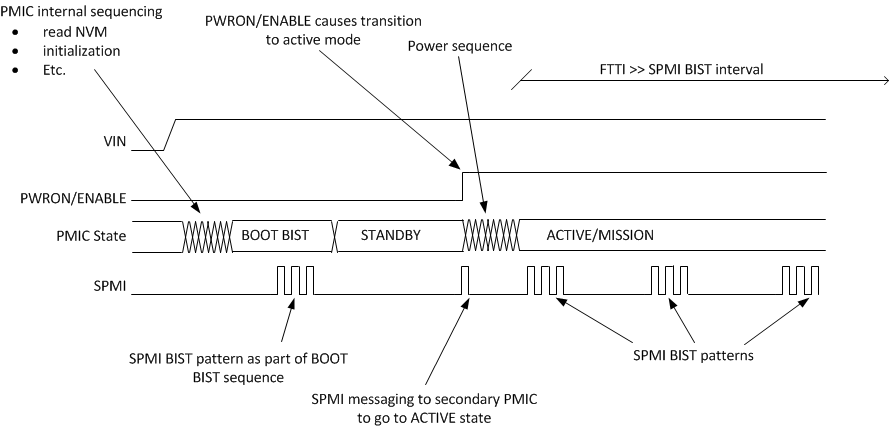
The SPMI-BIST is performed during BIST state and regularly during runtime operation. Figure 8-50 below illustrates how the SPMI-BIST operates during device power-up.
 Figure 8-50 SPMI-BIST
Operation
Figure 8-50 SPMI-BIST
OperationAfter the input power is detected and verified to be at the correct level, the TPS6594-Q1 initializes itself by reading the NVM and performs all actions that are needed to prepare for operation . After this initialization, the TPS6594-Q1 enters the BOOT BIST state, in which the internal logic performs a series of tests to verify that the TPS6594-Q1 device is OK. As part of this test, the SPMI- BIST is performed. After it is completed successfully, the TPS6594-Q1 device goes to the standby state and waits for further signals from the system to initiate the power-up sequence of the processor.
A valid on request initiates the processor power-up sequence. The controller device communicates this event through the SPMI bus to all of the target devices. After that, the power-up sequence is executed and TPS6594-Q1 enters the configured mission state.