JAJSCL2C October 2016 – August 2021 TPS65983B
PRODUCTION DATA
- 1 特長
- 2 アプリケーション
- 3 概要
- 4 Revision History
- 5 概要 (続き)
- 6 Pin Configuration and Functions
-
7 Specifications
- 7.1 Absolute Maximum Ratings
- 7.2 ESD Ratings
- 7.3 Recommended Operating Conditions
- 7.4 Thermal Information
- 7.5 Power Supply Requirements and Characteristics
- 7.6 Power Supervisor Characteristics
- 7.7 Power Consumption Characteristics
- 7.8 Cable Detection Characteristics
- 7.9 USB-PD Baseband Signal Requirements and Characteristics
- 7.10 USB-PD TX Driver Voltage Adjustment Parameter (1)
- 7.11 Port Power Switch Characteristics
- 7.12 Port Data Multiplexer Switching and Timing Characteristics
- 7.13 Port Data Multiplexer Clamp Characteristics
- 7.14 Port Data Multiplexer SBU Detection Requirements
- 7.15 Port Data Multiplexer Signal Monitoring Pullup and Pulldown Characteristics
- 7.16 Port Data Multiplexer USB Endpoint Requirements and Characteristics
- 7.17 Port Data Multiplexer BC1.2 Detection Requirements and Characteristics
- 7.18 Analog-to-Digital Converter (ADC) Characteristics
- 7.19 Input/Output (I/O) Requirements and Characteristics
- 7.20 I2C Slave Requirements and Characteristics
- 7.21 SPI Controller Characteristics
- 7.22 Single-Wire Debugger (SWD) Timing Requirements
- 7.23 BUSPOWERZ Configuration Requirements
- 7.24 HPD Timing Requirements and Characteristics
- 7.25 Thermal Shutdown Characteristics
- 7.26 Oscillator Requirements and Characteristics
- 7.27 Typical Characteristics
- 8 Parameter Measurement Information
-
9 Detailed Description
- 9.1 Overview
- 9.2 Functional Block Diagram
- 9.3
Feature Description
- 9.3.1 USB-PD Physical Layer
- 9.3.2 Cable Plug and Orientation Detection
- 9.3.3
Port Power Switches
- 9.3.3.1 5V Power Delivery
- 9.3.3.2 5V Power Switch as a Source
- 9.3.3.3 PP_5V0 Current Sense
- 9.3.3.4 PP_5V0 Current Limit
- 9.3.3.5 Internal HV Power Delivery
- 9.3.3.6 Internal HV Power Switch as a Source
- 9.3.3.7 Internal HV Power Switch as a Sink
- 9.3.3.8 Internal HV Power Switch Current Sense
- 9.3.3.9 Internal HV Power Switch Current Limit
- 9.3.3.10 External HV Power Delivery
- 9.3.3.11 External HV Power Switch as a Source with RSENSE
- 9.3.3.12 External HV Power Switch as a Sink with RSENSE
- 9.3.3.13 External HV Power Switch as a Sink without RSENSE
- 9.3.3.14 External Current Sense
- 9.3.3.15 External Current Limit
- 9.3.3.16 Soft Start
- 9.3.3.17 BUSPOWERZ
- 9.3.3.18 Voltage Transitions on VBUS through Port Power Switches
- 9.3.3.19 HV Transition to PP_RV0 Pull-Down on VBUS
- 9.3.3.20 VBUS Transition to VSAVE0V
- 9.3.3.21 C_CC1 and C_CC2 Power Configuration and Power Delivery
- 9.3.3.22 PP_CABLE to C_CC1 and C_CC2 Switch Architecture
- 9.3.3.23 PP_CABLE to C_CC1 and C_CC2 Current Limit
- 9.3.4
USB Type-C Port Data Multiplexer
- 9.3.4.1 USB Top and Bottom Ports
- 9.3.4.2 Multiplexer Connection Orientation
- 9.3.4.3 Digital Crossbar Multiplexer
- 9.3.4.4 SBU Crossbar Multiplexer
- 9.3.4.5 Signal Monitoring and Pullup and Pulldown
- 9.3.4.6 Port Multiplexer Clamp
- 9.3.4.7 USB2.0 Low-Speed Endpoint
- 9.3.4.8 Battery Charger (BC1.2) Detection Block
- 9.3.4.9 BC1.2 Data Contact Detect
- 9.3.4.10 BC1.2 Primary and Secondary Detection
- 9.3.5 Power Management
- 9.3.6 Digital Core
- 9.3.7 USB-PD BMC Modem Interface
- 9.3.8 System Glue Logic
- 9.3.9 Power Reset Congrol Module (PRCM)
- 9.3.10 Interrupt Monitor
- 9.3.11 ADC Sense
- 9.3.12 UART
- 9.3.13 I2C Slave
- 9.3.14 SPI Controller
- 9.3.15 Single-Wire Debugger Interface
- 9.3.16 DisplayPort HPD Timers
- 9.3.17 ADC
- 9.3.18 I/O Buffers
- 9.3.19 Thermal Shutdown
- 9.3.20 Oscillators
- 9.4 Device Functional Modes
- 9.5 Programming
-
10Application and Implementation
- 10.1 Application Information
- 10.2
Typical Application
- 10.2.1
Fully-Featured USB Type-C and PD Charger Application
- 10.2.1.1 Design Requirements
- 10.2.1.2
Detailed Design Procedure
- 10.2.1.2.1 TPS65983B External Flash
- 10.2.1.2.2 I2C (I2C), Debug Control (DEBUG_CTL), and Single-Wire De-bugger (SWD) Resistors
- 10.2.1.2.3 Oscillator (R_OSC) Resistor
- 10.2.1.2.4 VBUS Capacitor and Ferrite Bead
- 10.2.1.2.5 Soft Start (SS) Capacitor
- 10.2.1.2.6 USB Top (C_USB_T), USB Bottom (C_USB_B), and Sideband-Use (SBU) Connections
- 10.2.1.2.7 Port Power Switch (PP_EXT, PP_HV, PP_5V0, and PP_CABLE) Capacitors
- 10.2.1.2.8 Cable Connection (CCn) Capacitors and RPD_Gn Connections
- 10.2.1.2.9 LDO_3V3, LDO_1V8A, LDO_1V8D, LDO_BMC, VOUT_3V3, VIN_3V3, and VDDIO
- 10.2.1.3 Application Curve
- 10.2.2 Dual-Port Notebook Application Supporting USB PD Charging and DisplayPort
- 10.2.1
Fully-Featured USB Type-C and PD Charger Application
- 11Power Supply Recommendations
-
12Layout
- 12.1
Layout Guidelines
- 12.1.1 TPS65983B Recommended Footprints
- 12.1.2 Alternate TPS65983B Footprint (Oval Pads)
- 12.1.3 Top TPS65983B Placement and Bottom Component Placement and Layout
- 12.1.4 Oval Pad Footprint Layout and Placement
- 12.1.5 Component Placement
- 12.1.6 Designs Rules and Guidance
- 12.1.7 Routing PP_HV, PP_EXT, PP_5V0, and VBUS
- 12.1.8 Routing Top and Bottom Passive Components
- 12.1.9 Void Via Placement
- 12.1.10 Top Layer Routing
- 12.1.11 Inner Signal Layer Routing
- 12.1.12 Bottom Layer Routing
- 12.2 Layout Example
- 12.1
Layout Guidelines
- 13Device and Documentation Support
- 14Mechanical, Packaging, and Orderable Information
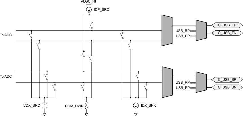
9.3.4.8 Battery Charger (BC1.2) Detection Block
The battery charger (BC1.2) detection block integrates circuitry to detect when the connected entity on the USB D+/D– pins is a charger. To enable the required detection mechanisms, the block integrates various voltage sources, currents, and resistances to the Port Data Multiplexers. Figure 9-39 shows the connections of these elements to the Port Data Multiplexers.
 Figure 9-39 BC1.2 Detection Circuitry