JAJSCL2C October 2016 – August 2021 TPS65983B
PRODUCTION DATA
- 1 特長
- 2 アプリケーション
- 3 概要
- 4 Revision History
- 5 概要 (続き)
- 6 Pin Configuration and Functions
-
7 Specifications
- 7.1 Absolute Maximum Ratings
- 7.2 ESD Ratings
- 7.3 Recommended Operating Conditions
- 7.4 Thermal Information
- 7.5 Power Supply Requirements and Characteristics
- 7.6 Power Supervisor Characteristics
- 7.7 Power Consumption Characteristics
- 7.8 Cable Detection Characteristics
- 7.9 USB-PD Baseband Signal Requirements and Characteristics
- 7.10 USB-PD TX Driver Voltage Adjustment Parameter (1)
- 7.11 Port Power Switch Characteristics
- 7.12 Port Data Multiplexer Switching and Timing Characteristics
- 7.13 Port Data Multiplexer Clamp Characteristics
- 7.14 Port Data Multiplexer SBU Detection Requirements
- 7.15 Port Data Multiplexer Signal Monitoring Pullup and Pulldown Characteristics
- 7.16 Port Data Multiplexer USB Endpoint Requirements and Characteristics
- 7.17 Port Data Multiplexer BC1.2 Detection Requirements and Characteristics
- 7.18 Analog-to-Digital Converter (ADC) Characteristics
- 7.19 Input/Output (I/O) Requirements and Characteristics
- 7.20 I2C Slave Requirements and Characteristics
- 7.21 SPI Controller Characteristics
- 7.22 Single-Wire Debugger (SWD) Timing Requirements
- 7.23 BUSPOWERZ Configuration Requirements
- 7.24 HPD Timing Requirements and Characteristics
- 7.25 Thermal Shutdown Characteristics
- 7.26 Oscillator Requirements and Characteristics
- 7.27 Typical Characteristics
- 8 Parameter Measurement Information
-
9 Detailed Description
- 9.1 Overview
- 9.2 Functional Block Diagram
- 9.3
Feature Description
- 9.3.1 USB-PD Physical Layer
- 9.3.2 Cable Plug and Orientation Detection
- 9.3.3
Port Power Switches
- 9.3.3.1 5V Power Delivery
- 9.3.3.2 5V Power Switch as a Source
- 9.3.3.3 PP_5V0 Current Sense
- 9.3.3.4 PP_5V0 Current Limit
- 9.3.3.5 Internal HV Power Delivery
- 9.3.3.6 Internal HV Power Switch as a Source
- 9.3.3.7 Internal HV Power Switch as a Sink
- 9.3.3.8 Internal HV Power Switch Current Sense
- 9.3.3.9 Internal HV Power Switch Current Limit
- 9.3.3.10 External HV Power Delivery
- 9.3.3.11 External HV Power Switch as a Source with RSENSE
- 9.3.3.12 External HV Power Switch as a Sink with RSENSE
- 9.3.3.13 External HV Power Switch as a Sink without RSENSE
- 9.3.3.14 External Current Sense
- 9.3.3.15 External Current Limit
- 9.3.3.16 Soft Start
- 9.3.3.17 BUSPOWERZ
- 9.3.3.18 Voltage Transitions on VBUS through Port Power Switches
- 9.3.3.19 HV Transition to PP_RV0 Pull-Down on VBUS
- 9.3.3.20 VBUS Transition to VSAVE0V
- 9.3.3.21 C_CC1 and C_CC2 Power Configuration and Power Delivery
- 9.3.3.22 PP_CABLE to C_CC1 and C_CC2 Switch Architecture
- 9.3.3.23 PP_CABLE to C_CC1 and C_CC2 Current Limit
- 9.3.4
USB Type-C Port Data Multiplexer
- 9.3.4.1 USB Top and Bottom Ports
- 9.3.4.2 Multiplexer Connection Orientation
- 9.3.4.3 Digital Crossbar Multiplexer
- 9.3.4.4 SBU Crossbar Multiplexer
- 9.3.4.5 Signal Monitoring and Pullup and Pulldown
- 9.3.4.6 Port Multiplexer Clamp
- 9.3.4.7 USB2.0 Low-Speed Endpoint
- 9.3.4.8 Battery Charger (BC1.2) Detection Block
- 9.3.4.9 BC1.2 Data Contact Detect
- 9.3.4.10 BC1.2 Primary and Secondary Detection
- 9.3.5 Power Management
- 9.3.6 Digital Core
- 9.3.7 USB-PD BMC Modem Interface
- 9.3.8 System Glue Logic
- 9.3.9 Power Reset Congrol Module (PRCM)
- 9.3.10 Interrupt Monitor
- 9.3.11 ADC Sense
- 9.3.12 UART
- 9.3.13 I2C Slave
- 9.3.14 SPI Controller
- 9.3.15 Single-Wire Debugger Interface
- 9.3.16 DisplayPort HPD Timers
- 9.3.17 ADC
- 9.3.18 I/O Buffers
- 9.3.19 Thermal Shutdown
- 9.3.20 Oscillators
- 9.4 Device Functional Modes
- 9.5 Programming
-
10Application and Implementation
- 10.1 Application Information
- 10.2
Typical Application
- 10.2.1
Fully-Featured USB Type-C and PD Charger Application
- 10.2.1.1 Design Requirements
- 10.2.1.2
Detailed Design Procedure
- 10.2.1.2.1 TPS65983B External Flash
- 10.2.1.2.2 I2C (I2C), Debug Control (DEBUG_CTL), and Single-Wire De-bugger (SWD) Resistors
- 10.2.1.2.3 Oscillator (R_OSC) Resistor
- 10.2.1.2.4 VBUS Capacitor and Ferrite Bead
- 10.2.1.2.5 Soft Start (SS) Capacitor
- 10.2.1.2.6 USB Top (C_USB_T), USB Bottom (C_USB_B), and Sideband-Use (SBU) Connections
- 10.2.1.2.7 Port Power Switch (PP_EXT, PP_HV, PP_5V0, and PP_CABLE) Capacitors
- 10.2.1.2.8 Cable Connection (CCn) Capacitors and RPD_Gn Connections
- 10.2.1.2.9 LDO_3V3, LDO_1V8A, LDO_1V8D, LDO_BMC, VOUT_3V3, VIN_3V3, and VDDIO
- 10.2.1.3 Application Curve
- 10.2.2 Dual-Port Notebook Application Supporting USB PD Charging and DisplayPort
- 10.2.1
Fully-Featured USB Type-C and PD Charger Application
- 11Power Supply Recommendations
-
12Layout
- 12.1
Layout Guidelines
- 12.1.1 TPS65983B Recommended Footprints
- 12.1.2 Alternate TPS65983B Footprint (Oval Pads)
- 12.1.3 Top TPS65983B Placement and Bottom Component Placement and Layout
- 12.1.4 Oval Pad Footprint Layout and Placement
- 12.1.5 Component Placement
- 12.1.6 Designs Rules and Guidance
- 12.1.7 Routing PP_HV, PP_EXT, PP_5V0, and VBUS
- 12.1.8 Routing Top and Bottom Passive Components
- 12.1.9 Void Via Placement
- 12.1.10 Top Layer Routing
- 12.1.11 Inner Signal Layer Routing
- 12.1.12 Bottom Layer Routing
- 12.2 Layout Example
- 12.1
Layout Guidelines
- 13Device and Documentation Support
- 14Mechanical, Packaging, and Orderable Information
9.4.1 Boot Code
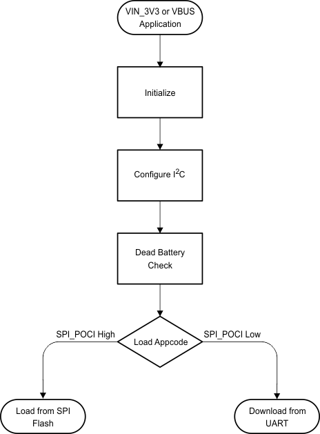
The TPS65983B has a Power-on-Reset (POR) circuit that monitors LDO_3V3 and issues an internal reset signal. The digital core, memory banks, and peripherals receive clock and RESET interrupt is issued to the digital core and the boot code starts executing. Figure 9-54 provides the TPS65983B boot code sequence.
The TPS65983B boot code is loaded from OTP on POR, and begins initializing TPS65983B settings. This initialization includes enabling and resetting internal registers, loading trim values, waiting for the trim values to settle, and configuring the device I2C addresses.
The unique I2C address is based on the customer programmable OTP, DEBUG_CTLX pins, and resistor configuration on the I2C_ADDR pin.
Once initial device configuration is complete the boot code determines if the TPS65983B is booting under dead battery condition (VIN_3V3 invalid, VBUS valid). If the boot code determines the TPS65983B is booting under dead battery condition, the BUSPOWERZ pin is sampled to determine the appropriate path for routing VBUS power to the system.
 Figure 9-54 Flow Diagram for Boot Code Sequence