JAJSCL2C October 2016 – August 2021 TPS65983B
PRODUCTION DATA
- 1 特長
- 2 アプリケーション
- 3 概要
- 4 Revision History
- 5 概要 (続き)
- 6 Pin Configuration and Functions
-
7 Specifications
- 7.1 Absolute Maximum Ratings
- 7.2 ESD Ratings
- 7.3 Recommended Operating Conditions
- 7.4 Thermal Information
- 7.5 Power Supply Requirements and Characteristics
- 7.6 Power Supervisor Characteristics
- 7.7 Power Consumption Characteristics
- 7.8 Cable Detection Characteristics
- 7.9 USB-PD Baseband Signal Requirements and Characteristics
- 7.10 USB-PD TX Driver Voltage Adjustment Parameter (1)
- 7.11 Port Power Switch Characteristics
- 7.12 Port Data Multiplexer Switching and Timing Characteristics
- 7.13 Port Data Multiplexer Clamp Characteristics
- 7.14 Port Data Multiplexer SBU Detection Requirements
- 7.15 Port Data Multiplexer Signal Monitoring Pullup and Pulldown Characteristics
- 7.16 Port Data Multiplexer USB Endpoint Requirements and Characteristics
- 7.17 Port Data Multiplexer BC1.2 Detection Requirements and Characteristics
- 7.18 Analog-to-Digital Converter (ADC) Characteristics
- 7.19 Input/Output (I/O) Requirements and Characteristics
- 7.20 I2C Slave Requirements and Characteristics
- 7.21 SPI Controller Characteristics
- 7.22 Single-Wire Debugger (SWD) Timing Requirements
- 7.23 BUSPOWERZ Configuration Requirements
- 7.24 HPD Timing Requirements and Characteristics
- 7.25 Thermal Shutdown Characteristics
- 7.26 Oscillator Requirements and Characteristics
- 7.27 Typical Characteristics
- 8 Parameter Measurement Information
-
9 Detailed Description
- 9.1 Overview
- 9.2 Functional Block Diagram
- 9.3
Feature Description
- 9.3.1 USB-PD Physical Layer
- 9.3.2 Cable Plug and Orientation Detection
- 9.3.3
Port Power Switches
- 9.3.3.1 5V Power Delivery
- 9.3.3.2 5V Power Switch as a Source
- 9.3.3.3 PP_5V0 Current Sense
- 9.3.3.4 PP_5V0 Current Limit
- 9.3.3.5 Internal HV Power Delivery
- 9.3.3.6 Internal HV Power Switch as a Source
- 9.3.3.7 Internal HV Power Switch as a Sink
- 9.3.3.8 Internal HV Power Switch Current Sense
- 9.3.3.9 Internal HV Power Switch Current Limit
- 9.3.3.10 External HV Power Delivery
- 9.3.3.11 External HV Power Switch as a Source with RSENSE
- 9.3.3.12 External HV Power Switch as a Sink with RSENSE
- 9.3.3.13 External HV Power Switch as a Sink without RSENSE
- 9.3.3.14 External Current Sense
- 9.3.3.15 External Current Limit
- 9.3.3.16 Soft Start
- 9.3.3.17 BUSPOWERZ
- 9.3.3.18 Voltage Transitions on VBUS through Port Power Switches
- 9.3.3.19 HV Transition to PP_RV0 Pull-Down on VBUS
- 9.3.3.20 VBUS Transition to VSAVE0V
- 9.3.3.21 C_CC1 and C_CC2 Power Configuration and Power Delivery
- 9.3.3.22 PP_CABLE to C_CC1 and C_CC2 Switch Architecture
- 9.3.3.23 PP_CABLE to C_CC1 and C_CC2 Current Limit
- 9.3.4
USB Type-C Port Data Multiplexer
- 9.3.4.1 USB Top and Bottom Ports
- 9.3.4.2 Multiplexer Connection Orientation
- 9.3.4.3 Digital Crossbar Multiplexer
- 9.3.4.4 SBU Crossbar Multiplexer
- 9.3.4.5 Signal Monitoring and Pullup and Pulldown
- 9.3.4.6 Port Multiplexer Clamp
- 9.3.4.7 USB2.0 Low-Speed Endpoint
- 9.3.4.8 Battery Charger (BC1.2) Detection Block
- 9.3.4.9 BC1.2 Data Contact Detect
- 9.3.4.10 BC1.2 Primary and Secondary Detection
- 9.3.5 Power Management
- 9.3.6 Digital Core
- 9.3.7 USB-PD BMC Modem Interface
- 9.3.8 System Glue Logic
- 9.3.9 Power Reset Congrol Module (PRCM)
- 9.3.10 Interrupt Monitor
- 9.3.11 ADC Sense
- 9.3.12 UART
- 9.3.13 I2C Slave
- 9.3.14 SPI Controller
- 9.3.15 Single-Wire Debugger Interface
- 9.3.16 DisplayPort HPD Timers
- 9.3.17 ADC
- 9.3.18 I/O Buffers
- 9.3.19 Thermal Shutdown
- 9.3.20 Oscillators
- 9.4 Device Functional Modes
- 9.5 Programming
-
10Application and Implementation
- 10.1 Application Information
- 10.2
Typical Application
- 10.2.1
Fully-Featured USB Type-C and PD Charger Application
- 10.2.1.1 Design Requirements
- 10.2.1.2
Detailed Design Procedure
- 10.2.1.2.1 TPS65983B External Flash
- 10.2.1.2.2 I2C (I2C), Debug Control (DEBUG_CTL), and Single-Wire De-bugger (SWD) Resistors
- 10.2.1.2.3 Oscillator (R_OSC) Resistor
- 10.2.1.2.4 VBUS Capacitor and Ferrite Bead
- 10.2.1.2.5 Soft Start (SS) Capacitor
- 10.2.1.2.6 USB Top (C_USB_T), USB Bottom (C_USB_B), and Sideband-Use (SBU) Connections
- 10.2.1.2.7 Port Power Switch (PP_EXT, PP_HV, PP_5V0, and PP_CABLE) Capacitors
- 10.2.1.2.8 Cable Connection (CCn) Capacitors and RPD_Gn Connections
- 10.2.1.2.9 LDO_3V3, LDO_1V8A, LDO_1V8D, LDO_BMC, VOUT_3V3, VIN_3V3, and VDDIO
- 10.2.1.3 Application Curve
- 10.2.2 Dual-Port Notebook Application Supporting USB PD Charging and DisplayPort
- 10.2.1
Fully-Featured USB Type-C and PD Charger Application
- 11Power Supply Recommendations
-
12Layout
- 12.1
Layout Guidelines
- 12.1.1 TPS65983B Recommended Footprints
- 12.1.2 Alternate TPS65983B Footprint (Oval Pads)
- 12.1.3 Top TPS65983B Placement and Bottom Component Placement and Layout
- 12.1.4 Oval Pad Footprint Layout and Placement
- 12.1.5 Component Placement
- 12.1.6 Designs Rules and Guidance
- 12.1.7 Routing PP_HV, PP_EXT, PP_5V0, and VBUS
- 12.1.8 Routing Top and Bottom Passive Components
- 12.1.9 Void Via Placement
- 12.1.10 Top Layer Routing
- 12.1.11 Inner Signal Layer Routing
- 12.1.12 Bottom Layer Routing
- 12.2 Layout Example
- 12.1
Layout Guidelines
- 13Device and Documentation Support
- 14Mechanical, Packaging, and Orderable Information
9.3.18.1 IOBUF_GPIOLS and IOBUF_GPIOLSI2C
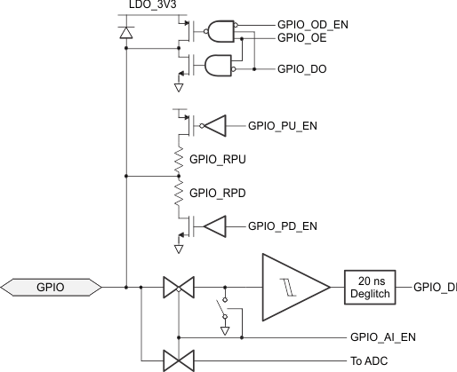
Figure 9-45 shows the GPIO I/O buffer for all GPIOn pins listed GPIO0-GPIO17 in Pin Configuration and Functions. GPIOn pins can be mapped to USB Type-C, USB PD, and application-specific events to control other ICs, interrupt a host processor, or receive input from another IC. This buffer is configurable to be a push-pull output, a weak push-pull, or open drain output. When configured as an input, the signal can be a deglitched digital input or an analog input to the ADC. The push-pull output is a simple CMOS output with independent pulldown control allowing open-drain connections. The weak push-pull is also a CMOS output, but with GPIO_RPU resistance in series with the drain. The supply voltage to this buffer is configurable to be LDO_3V3 by default or VDDIO. For simplicity, the connection to VDDIO is not shown in Figure 9-45, but the connection to VDDIO is fail-safe and a diode will not be present from GPIOn to VDDIO in this configuration. The pullup and pulldown output drivers are independently controlled from the input and are enabled or disabled via application code in the digital core.
 Figure 9-45 IOBUF_GPIOLS (General GPIO) I/O
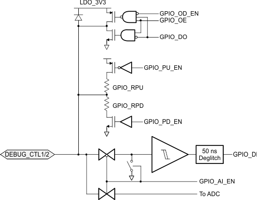
Figure 9-46 shows the IOBUF_GPIOLSI2C that is identical to IOBUF_GPIOLS with an extended deglitch time.
 Figure 9-46 IOBUF_GPIOLSI2C (General GPIO) I/O with I2C Deglitch