JAJSCL2C October 2016 – August 2021 TPS65983B
PRODUCTION DATA
- 1 特長
- 2 アプリケーション
- 3 概要
- 4 Revision History
- 5 概要 (続き)
- 6 Pin Configuration and Functions
-
7 Specifications
- 7.1 Absolute Maximum Ratings
- 7.2 ESD Ratings
- 7.3 Recommended Operating Conditions
- 7.4 Thermal Information
- 7.5 Power Supply Requirements and Characteristics
- 7.6 Power Supervisor Characteristics
- 7.7 Power Consumption Characteristics
- 7.8 Cable Detection Characteristics
- 7.9 USB-PD Baseband Signal Requirements and Characteristics
- 7.10 USB-PD TX Driver Voltage Adjustment Parameter (1)
- 7.11 Port Power Switch Characteristics
- 7.12 Port Data Multiplexer Switching and Timing Characteristics
- 7.13 Port Data Multiplexer Clamp Characteristics
- 7.14 Port Data Multiplexer SBU Detection Requirements
- 7.15 Port Data Multiplexer Signal Monitoring Pullup and Pulldown Characteristics
- 7.16 Port Data Multiplexer USB Endpoint Requirements and Characteristics
- 7.17 Port Data Multiplexer BC1.2 Detection Requirements and Characteristics
- 7.18 Analog-to-Digital Converter (ADC) Characteristics
- 7.19 Input/Output (I/O) Requirements and Characteristics
- 7.20 I2C Slave Requirements and Characteristics
- 7.21 SPI Controller Characteristics
- 7.22 Single-Wire Debugger (SWD) Timing Requirements
- 7.23 BUSPOWERZ Configuration Requirements
- 7.24 HPD Timing Requirements and Characteristics
- 7.25 Thermal Shutdown Characteristics
- 7.26 Oscillator Requirements and Characteristics
- 7.27 Typical Characteristics
- 8 Parameter Measurement Information
-
9 Detailed Description
- 9.1 Overview
- 9.2 Functional Block Diagram
- 9.3
Feature Description
- 9.3.1 USB-PD Physical Layer
- 9.3.2 Cable Plug and Orientation Detection
- 9.3.3
Port Power Switches
- 9.3.3.1 5V Power Delivery
- 9.3.3.2 5V Power Switch as a Source
- 9.3.3.3 PP_5V0 Current Sense
- 9.3.3.4 PP_5V0 Current Limit
- 9.3.3.5 Internal HV Power Delivery
- 9.3.3.6 Internal HV Power Switch as a Source
- 9.3.3.7 Internal HV Power Switch as a Sink
- 9.3.3.8 Internal HV Power Switch Current Sense
- 9.3.3.9 Internal HV Power Switch Current Limit
- 9.3.3.10 External HV Power Delivery
- 9.3.3.11 External HV Power Switch as a Source with RSENSE
- 9.3.3.12 External HV Power Switch as a Sink with RSENSE
- 9.3.3.13 External HV Power Switch as a Sink without RSENSE
- 9.3.3.14 External Current Sense
- 9.3.3.15 External Current Limit
- 9.3.3.16 Soft Start
- 9.3.3.17 BUSPOWERZ
- 9.3.3.18 Voltage Transitions on VBUS through Port Power Switches
- 9.3.3.19 HV Transition to PP_RV0 Pull-Down on VBUS
- 9.3.3.20 VBUS Transition to VSAVE0V
- 9.3.3.21 C_CC1 and C_CC2 Power Configuration and Power Delivery
- 9.3.3.22 PP_CABLE to C_CC1 and C_CC2 Switch Architecture
- 9.3.3.23 PP_CABLE to C_CC1 and C_CC2 Current Limit
- 9.3.4
USB Type-C Port Data Multiplexer
- 9.3.4.1 USB Top and Bottom Ports
- 9.3.4.2 Multiplexer Connection Orientation
- 9.3.4.3 Digital Crossbar Multiplexer
- 9.3.4.4 SBU Crossbar Multiplexer
- 9.3.4.5 Signal Monitoring and Pullup and Pulldown
- 9.3.4.6 Port Multiplexer Clamp
- 9.3.4.7 USB2.0 Low-Speed Endpoint
- 9.3.4.8 Battery Charger (BC1.2) Detection Block
- 9.3.4.9 BC1.2 Data Contact Detect
- 9.3.4.10 BC1.2 Primary and Secondary Detection
- 9.3.5 Power Management
- 9.3.6 Digital Core
- 9.3.7 USB-PD BMC Modem Interface
- 9.3.8 System Glue Logic
- 9.3.9 Power Reset Congrol Module (PRCM)
- 9.3.10 Interrupt Monitor
- 9.3.11 ADC Sense
- 9.3.12 UART
- 9.3.13 I2C Slave
- 9.3.14 SPI Controller
- 9.3.15 Single-Wire Debugger Interface
- 9.3.16 DisplayPort HPD Timers
- 9.3.17 ADC
- 9.3.18 I/O Buffers
- 9.3.19 Thermal Shutdown
- 9.3.20 Oscillators
- 9.4 Device Functional Modes
- 9.5 Programming
-
10Application and Implementation
- 10.1 Application Information
- 10.2
Typical Application
- 10.2.1
Fully-Featured USB Type-C and PD Charger Application
- 10.2.1.1 Design Requirements
- 10.2.1.2
Detailed Design Procedure
- 10.2.1.2.1 TPS65983B External Flash
- 10.2.1.2.2 I2C (I2C), Debug Control (DEBUG_CTL), and Single-Wire De-bugger (SWD) Resistors
- 10.2.1.2.3 Oscillator (R_OSC) Resistor
- 10.2.1.2.4 VBUS Capacitor and Ferrite Bead
- 10.2.1.2.5 Soft Start (SS) Capacitor
- 10.2.1.2.6 USB Top (C_USB_T), USB Bottom (C_USB_B), and Sideband-Use (SBU) Connections
- 10.2.1.2.7 Port Power Switch (PP_EXT, PP_HV, PP_5V0, and PP_CABLE) Capacitors
- 10.2.1.2.8 Cable Connection (CCn) Capacitors and RPD_Gn Connections
- 10.2.1.2.9 LDO_3V3, LDO_1V8A, LDO_1V8D, LDO_BMC, VOUT_3V3, VIN_3V3, and VDDIO
- 10.2.1.3 Application Curve
- 10.2.2 Dual-Port Notebook Application Supporting USB PD Charging and DisplayPort
- 10.2.1
Fully-Featured USB Type-C and PD Charger Application
- 11Power Supply Recommendations
-
12Layout
- 12.1
Layout Guidelines
- 12.1.1 TPS65983B Recommended Footprints
- 12.1.2 Alternate TPS65983B Footprint (Oval Pads)
- 12.1.3 Top TPS65983B Placement and Bottom Component Placement and Layout
- 12.1.4 Oval Pad Footprint Layout and Placement
- 12.1.5 Component Placement
- 12.1.6 Designs Rules and Guidance
- 12.1.7 Routing PP_HV, PP_EXT, PP_5V0, and VBUS
- 12.1.8 Routing Top and Bottom Passive Components
- 12.1.9 Void Via Placement
- 12.1.10 Top Layer Routing
- 12.1.11 Inner Signal Layer Routing
- 12.1.12 Bottom Layer Routing
- 12.2 Layout Example
- 12.1
Layout Guidelines
- 13Device and Documentation Support
- 14Mechanical, Packaging, and Orderable Information
10.2.2.2.3 9.3.2.3 DC Barrel Jack and Type-C PD Charging
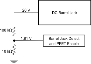
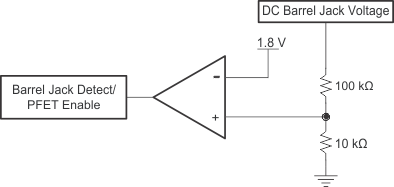
The system is design to either charge over Type-C or from the DC barrel jack. The TPS65983B detects that the DC barrel jack is connected to GPIOn. In the simplest form, a voltage divider could be set to the GPIO I/O level when the DC Barrel jack voltage is present, as shown in Figure 10-4. A comparator circuit is recommend and used in this design for design robustness, as shown in Figure 10-5.
 Figure 10-4 DC Barrel Jack Voltage Divider
 Figure 10-5 Barrel Jack Detect Comparator
This detect signal is used to determine if the barrel jack is present to support the 20-V PD power contracts and to hand-off charging from barrel jack to Type-C or Type-C to barrel jack. When the DC barrel jack is detected the TPS65983B at each Type-C port will not request 20 V for charging and the system will be able to support a 20 V source power contract to another device. When the DC Barrel Jack is disconnected the TPS65983B will exit any 20-V source power contract and renegotiate a power contract. When the DC Barrel Jack is connected the TPS65983B will send updated source capabilities and renegotiate a power contract if needed.
The PFET enable will be controlled by the DC barrel jack detect comparator depicted in Figure 10-5. This will allow the system to power up from dead battery through the barrel jack as well as the Type-C ports. Figure 10-6 shows the flow between changing from DC barrel jack charging and USB-PD charging. The example uses back-to-back PFETs for disabling and enabling the power path for the DC Barrel Jack. It is important to use PFETs that are rated above the specified parameters to ensure robustness of the system. The DC Barrel Jack voltage in this design is assumed to be 20 V at 5 A, so the PFETs are recommended to be rated at a minimum of 30 V and 10 A of current.
The TPS65983B in this design also provides the GPIO control for the PFET gate drive that passes the DC Barrel Jack Voltage to the system. Figure 10-6 shows the flow between changing from DC Barrel Jack charging and Type-C PD charging.