SLVSAJ4C September 2010 – October 2017
PRODUCTION DATA.
6 Specifications
6.1 Absolute Maximum Ratings
over operating free-air temperature range (unless otherwise noted)(1)(2)| MIN | MAX | UNIT | ||
|---|---|---|---|---|
| Input voltage range, VIN | –11 | 0.3 | V | |
| Noise reduction pin voltage range, VNR | –11 | 5.5 | V | |
| Enable voltage range, VEN | –VIN | 5.5 | V | |
| Output current, IOUT | Internally limited | |||
| Output short-circuit duration | Indefinite | |||
| Continuous total power dissipation, PD | See the Power Dissipation Ratings table | |||
| Latch-up performance meets 100 mA per AEC-Q100 | Class I | 100 | mA | ||
| Junction temperature range, TJ | –55 | 150 | °C | |
| Storage temperature, Tstg | –65 | 150 | °C | |
(1) Stresses beyond those listed under Absolute Maximum Ratings may cause permanent damage to the device. These are stress ratings only, which do not imply functional operation of the device at these or any other conditions beyond those indicated under Recommended Operating Conditions. Exposure to absolute-maximum-rated conditions for extended periods may affect device reliability.
(2) All voltage values are with respect to network ground terminal.
6.2 ESD Ratings
| VALUE | UNIT | |||
|---|---|---|---|---|
| V(ESD) | Electrostatic discharge | Human-body model (HBM), per AEC Q100-002(1) | ±2000 | V |
| Charged-device model (CDM), per AEC Q100-011 | ±500 | |||
| Machine model | ±200 | |||
(1) AEC Q100-002 indicates that HBM stressing shall be in accordance with the ANSI/ESDA/JEDEC JS-001 specification.
6.3 Power Dissipation Ratings
| BOARD | PACKAGE | RθJC | RθJA | DERATING FACTOR ABOVE TA = 25°C |
TA ≤ 25°C POWER RATING |
TA = 70°C POWER RATING |
TA = 85°C POWER RATING |
|---|---|---|---|---|---|---|---|
| Low-K(1) | DBV | 64°C/W | 255°C/W | 3.9 mW/°C | 390 mW | 215 mW | 155 mW |
| High-K(2) | DBV | 64°C/W | 180°C/W | 5.6 mW/°C | 560 mW | 310 mW | 225 mW |
(1) The JEDEC low-K (1s) board design used to derive this data was a 3-inch × 3- inch (7,62-cm × 7,62-cm), two-layer board with 2-ounce (0.071-mm thick) copper traces on top of the board.
(2) The JEDEC High-K (2s2p) board design used to derive this data was a 3 inch × 3 inch (7,62-cm × 7,62-cm), multilayer board with 1-ounce (0.035-mm thick) internal power and ground planes and 2-ounce (0.071-mm thick) copper traces on the top and bottom of the board.
6.4 Electrical Characteristics
Over operating junction temperature range, VIN = VOUTnom – 0.5V, IOUT = 1mA, VEN = 1.5V, COUT = 2.2μF, and CNR = 0.01μF, unless otherwise noted. Typical values are at TJ = 25°C.| PARAMETER | TEST CONDITIONS | MIN | TYP | MAX | UNIT | ||
|---|---|---|---|---|---|---|---|
| VIN | Input voltage range(1) | –10 | –2.7 | V | |||
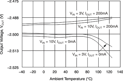
| VOUT | Accuracy | Nominal | TJ = 25°C | –1% | 1% | ||
| TPS723xx-Q1 versus VIN / IOUT / T |
–10V ≤ VIN ≤ VOUT – 0.5V, 10 μA ≤ IOUT ≤ 200 mA |
–2% | ±1% | 2% | |||
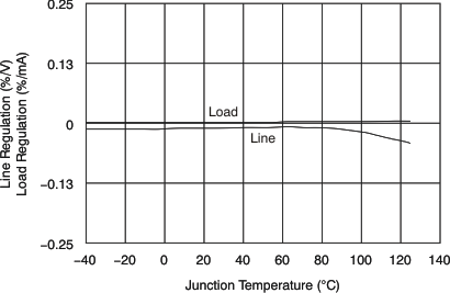
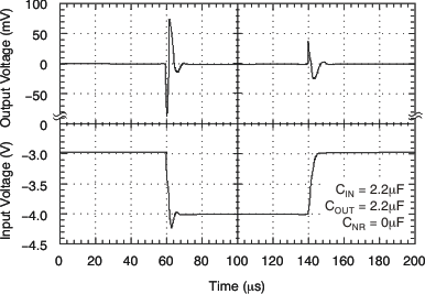
| VOUT% / VIN | Line regulation | –10 V ≤ VIN ≤ VOUT(nom) – 0.5 V | 0.04 | %/V | |||
| VOUT% / IOUT | Load regulation | 0 mA ≤ IOUT ≤ 200 mA | 0.002 | %/mA | |||
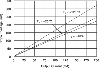
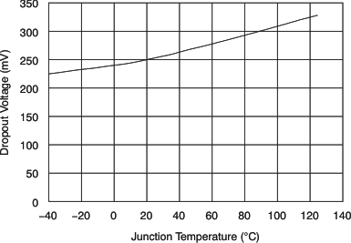
| VDO | Dropout voltage at VOUT = 0.96 × VOUTnom | IOUT = 200 mA | 280 | 500 | mV | ||
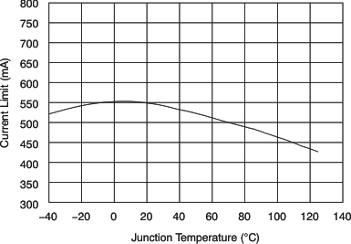
| ICL | Current limit | VOUT = 0.85 × VOUT(nom) | 300 | 550 | 800 | mA | |
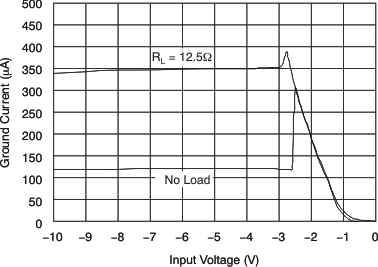
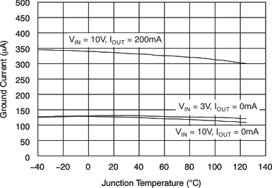
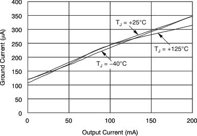
| IGND | Ground pin current | IOUT = 0 mA (IQ), –10 V ≤ VIN ≤ VOUT – 0.5 V |
130 | 200 | μA | ||
| IOUT = 200 mA, –10 V ≤ VIN ≤ VOUT – 0.5 V |
350 | 500 | |||||
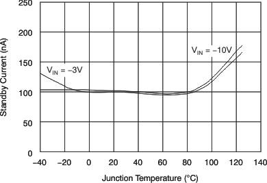
| ISHDN | Shutdown ground pin current | –0.4 V ≤ VEN ≤ 0.4 V, –10V ≤ VIN ≤ VOUT – 0.5 V |
0.1 | 2 | μA | ||
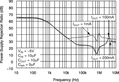
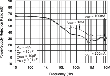
| PSRR | Power-supply rejection ratio | IOUT = 200 mA, 1 kHz, CIN = COUT = 10 μF |
65 | dB | |||
| IOUT = 200 mA, 10 kHz, CIN = COUT = 10 μF |
48 | ||||||
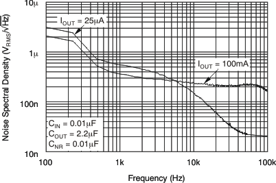
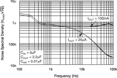
| Vn | Output noise voltage | COUT = 10 μF, 10 Hz to 100 kHz, IOUT = 200 mA |
60 | μVRMS | |||
| tSTR | Startup time | VOUT = –2.5 V, COUT = 1 μF, RL = 25 Ω |
1 | ms | |||
| VEN(HI) | Enable threshold positive | 1.5 | V | ||||
| VEN(LO) | Enable threshold negative | –1.5 | V | ||||
| VDIS(HI) | Disable threshold positive | 0.4 | V | ||||
| VDIS(LO) | Disable threshold negative | –0.4 | V | ||||
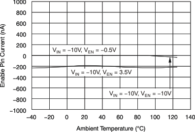
| IEN | Enable pin current | –10 V ≤ VIN ≤ VOUT – 0.5 V, –10 V ≤ VEN ≤ ±3.5 V |
0.1 | 2 | μA | ||
| TSD | Thermal shutdown temperature | Shutdown, temperature increasing | 165 | °C | |||
| Reset, temperature decreasing | 145 | ||||||
| TJ | Operating junction temperature | –40 | 125 | °C | |||
(1) Maximum VIN = (VOUT – VDO) or – 2.7 V, whichever is more negative.
6.5 Typical Characteristics
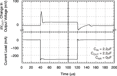
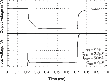
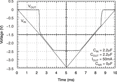
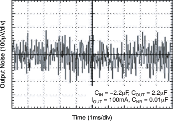
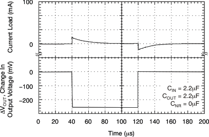
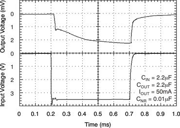
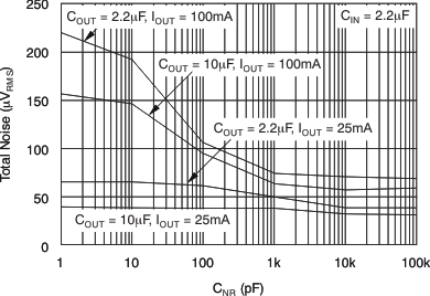
TPS723xx-Q1 at VIN = VOUTnom – 0.5 V, IOUT = 1 mA, VEN = 1.5 V, COUT = 2.2 μF, and CNR = 0.01 μF, unless otherwise noted.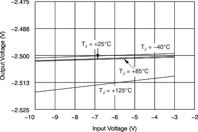
(10 Hz to 100 kHz)
