JAJSEP4C June   2018  – May 2022 TPS746-Q1

PRODUCTION DATA  

  1. 特長
  2. アプリケーション
  3. 概要
  4. Revision History
  5. Pin Configuration and Functions
  6. Specifications
    1. 6.1 Absolute Maximum Ratings
    2. 6.2 ESD Ratings
    3. 6.3 Recommended Operating Conditions
    4. 6.4 Thermal Information
    5. 6.5 Electrical Characteristics
    6. 6.6 Timing Requirements
    7. 6.7 Typical Characteristics
  7. Detailed Description
    1. 7.1 Overview
    2. 7.2 Functional Block Diagrams
    3. 7.3 Feature Description
      1. 7.3.1 Undervoltage Lockout (UVLO)
      2. 7.3.2 Shutdown
      3. 7.3.3 Foldback Current Limit
      4. 7.3.4 Thermal Shutdown
    4. 7.4 Device Functional Modes
      1. 7.4.1 Device Functional Mode Comparison
      2. 7.4.2 Normal Operation
      3. 7.4.3 Dropout Operation
      4. 7.4.4 Disabled
  8. Application and Implementation
    1. 8.1 Application Information
      1. 8.1.1 Adjustable Device Feedback Resistors
      2. 8.1.2 Input and Output Capacitor Selection
      3. 8.1.3 Dropout Voltage
      4. 8.1.4 Exiting Dropout
      5. 8.1.5 Reverse Current
      6. 8.1.6 Power Dissipation (PD)
      7. 8.1.7 Power-Good Function
      8. 8.1.8 Feed-Forward Capacitor (CFF)
      9. 8.1.9 Start-Up Sequencing
    2. 8.2 Typical Application
      1. 8.2.1 Design Requirements
      2. 8.2.2 Detailed Design Procedure
        1. 8.2.2.1 Input Current
        2. 8.2.2.2 Thermal Dissipation
      3. 8.2.3 Application Curve
  9. Power Supply Recommendations
  10. 10Layout
    1. 10.1 Layout Guidelines
    2. 10.2 Layout Examples
  11. 11Device and Documentation Support
    1. 11.1 Device Support
      1. 11.1.1 Device Nomenclature
    2. 11.2 Documentation Support
      1. 11.2.1 Related Documentation
    3. 11.3 Receiving Notification of Documentation Updates
    4. 11.4 サポート・リソース
    5. 11.5 Trademarks
    6. 11.6 Electrostatic Discharge Caution
    7. 11.7 Glossary
      1.      Mechanical, Packaging, and Orderable Information

パッケージ・オプション

メカニカル・データ(パッケージ|ピン)
サーマルパッド・メカニカル・データ
発注情報

Adjustable Device Feedback Resistors

Figure 8-1 shows that the output voltage of the TPS746P-Q1 can be adjusted from 0.55 V to 5.5 V by using a resistor divider network.
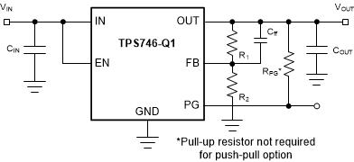
GUID-228B4C52-DD90-4A2F-8505-4D87FC3D092F-low.gifFigure 8-1 Adjustable Operation

The adjustable-version device requires external feedback divider resistors to set the output voltage. VOUT is set using the feedback divider resistors, R1 and R2, according to the following equation:

Equation 2. VOUT = VFB × (1 + R1 / R2)

To ignore the FB pin current error term in the VOUT equation, set the feedback divider current to 100x the FB pin current listed in the Electrical Characteristics table. This setting provides the maximum feedback divider series resistance, as shown in the following equation:

Equation 3. R1 + R2 ≤ VOUT / (IFB × 100)