-
TPS797xx Ultra-Low IQ, 50-mA Low-Dropout Linear Regulators With Power Good Output in SC70 Package
- 1 Features
- 2 Applications
- 3 Description
- 4 Revision History
- 5 Pin Configuration and Functions
- 6 Specifications
- 7 Detailed Description
- 8 Application and Implementation
- 9 Power-Supply Recommendations
- 10Layout
- 11Device and Documentation Support
- 12Mechanical, Packaging, and Orderable Information
- IMPORTANT NOTICE
TPS797xx Ultra-Low IQ, 50-mA Low-Dropout Linear Regulators With Power Good Output in SC70 Package
1 Features
- 50-mA Low-Dropout Regulator
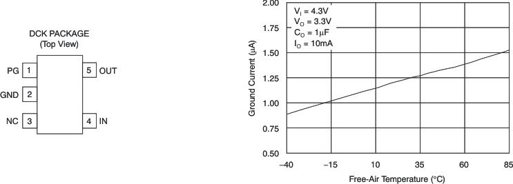
- Ultra-Low 1.2-µA Quiescent Current at 10 mA
- 5-Pin SC70 (DCK) Package
- Integrated Power Good Output
- Stable With Any Capacitor Greater Than 0.47 µF
- Typical Dropout Voltage of 105 mV at 10 mA (TPS79733)
- Over-Current Limitation
- Operating Junction Temperature Range of –40°C to 85°C
2 Applications
- Battery-Powered Microcontrollers and Microprocessors
3 Description
The TPS797xx family of low-dropout voltage regulators (LDOs) offers the benefits of low-dropout voltage and ultra-low-power operation. The device is stable with any capacitor greater than 0.47-µF. Therefore, implementations of this device require very little board space due to the miniaturized packaging and potentially small output capacitor. In addition, the family includes an integrated open drain active-high power good (PG) output. Intended for use in microcontroller-based, battery-powered applications, the TPS797xx family low dropout and ultra-low-power operation result in a significant increase in system battery operating life. The small packaging minimizes consumption of board space.
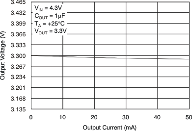
The device is enabled when the applied voltage exceeds the minimum input voltage. The usual PNP pass transistor has been replaced by a PMOS pass element. Because the PMOS pass element behaves as a low-value resistor, the dropout voltage is very low (typically, 105 mV at 10-mA of load current), and is directly proportional to the load current. The quiescent current is ultra-low (1.2-µA, typically) and is stable over the entire range of output load current
(0 mA to 50 mA). When properly configured with a pullup resistor, the PG output can implement a power-on reset or low-battery indicator.
Device Information(1)
| PART NUMBER | PACKAGE | BODY SIZE (NOM) |
|---|---|---|
| TPS797xx | SC70 (5) | 2.00 mm × 1.25 mm |
- For all available packages, see the orderable addendum at the end of the data sheet.
Ground Current vs Free-Air Temperature

4 Revision History
Changes from I Revision (October 2013) to J Revision
- Added ESD Ratings table, Feature Description section, Device Functional Modes, Application and Implementation section, Power Supply Recommendations section, Layout section, Device and Documentation Support section, and Mechanical, Packaging, and Orderable Information sectionGo
- Deleted Dissipation Ratings table; see Thermal Information tableGo
- Added Thermal Information tableGo
- Changed Load Regulation parameter unit From: mV To: %/AGo
- Changed Output Spectral Noise Density vs Frequency graph Y-axis unit From: nV/√Hz To: µV/√HzGo
- Changed IOUTx values From: ICL To: ISCGo
Changes from H Revision (April 2012) to I Revision
- Changed Dropout Voltage vs Junction Temperature graph Y-axis unit From: V To: mV (typo)Go
Changes from G Revision (November 2009) to H Revision
- Deleted sentence regarding thermal protectionGo
Changes from F Revision (May 2009) to G Revision
- Changed document titleGo
- Deleted references to SOT323 package throughout documentGo
- Changed Test Conditions for Electrical Characteristics tableGo
- Changed output voltage accuracy test conditions from 10 µA < IOUT < 10 mA to 1 mA < IOUT < 10 mAGo
- Deleted line regulation maximum specificationGo
- Changed PG trip threshold voltage test conditions from VOUT decreasing to VOUT increasing; deleted minimum and maximum specificationsGo
- Revised PG low output low voltage test conditionsGo
- Updated PG leakage current test conditionsGo
5 Pin Configuration and Functions

Pin Functions
| PIN | I/O | DESCRIPTION | |
|---|---|---|---|
| NO. | NAME | ||
| 1 | PG | O | The PG pin for the fixed voltage option devices is an open drain, active-high output that indicates the status of VO (output of the LDO). When VO exceeds approximately 90% of the regulated voltage, PG goes to a high-impedance state. PG goes to a low-impedance state when VO falls below approximately 90% (that is, overload condition) of the regulated voltage. The open drain output of the PG pin requires a pullup resistor. |
| 2 | GND | — | Ground |
| 3 | NC | — | No connection |
| 4 | IN | I | The IN pin is the power-supply input to the device. |
| 5 | OUT | O | The OUT pin provides the regulated output voltage of the device. |
6 Specifications
6.1 Absolute Maximum Ratings
over operating free-air temperature range (unless otherwise noted) (1)| MIN | MAX | UNIT | ||
|---|---|---|---|---|
| Voltage | Input voltage(2) | –0.3 | 6 | V |
| Maximum dc output voltage | 4.9 | V | ||
| Current | Peak output current | Internally limited | A | |
| Temperature | Operating virtual junction temperature, TJ | –40 | 85 | °C |
| Storage temperature, Tstg | –65 | 150 | °C | |
6.2 ESD Ratings
| VALUE | UNIT | |||
|---|---|---|---|---|
| V(ESD) | Electrostatic discharge | Human-body model (HBM), per ANSI/ESDA/JEDEC JS-001(1) | ±2000 | V |
| Charged-device model (CDM), per JEDEC specification JESD22-C101(2) | ±500 | |||
6.3 Recommended Operating Conditions
over operating free-air temperature range (unless otherwise noted)| MIN | NOM | MAX | UNIT | ||
|---|---|---|---|---|---|
| VI | Input voltage | 1.8 | 5.5 | V | |
| VO | Output voltage | 1.8 | 3.3 | V | |
| IO | Output current | 0 | 50 | mA | |
| CI | Input capacitor | 0 | 0.1 | µF | |
| CO | Output capacitor | 0.47 | 1 | µF | |
| TJ | Junction temperature | –40 | 85 | °C | |
6.4 Thermal Information
| THERMAL METRIC(1) | TPS797xx | UNIT | |
|---|---|---|---|
| DCK (SC70) | |||
| 5 PINS | |||
| RθJA | Junction-to-ambient thermal resistance | 230.9 | °C/W |
| RθJC(top) | Junction-to-case (top) thermal resistance | 98.3 | °C/W |
| RθJB | Junction-to-board thermal resistance | 70.7 | °C/W |
| ψJT | Junction-to-top characterization parameter | 3.9 | °C/W |
| ψJB | Junction-to-board characterization parameter | 70.1 | °C/W |
| RθJC(bot) | Junction-to-case (bottom) thermal resistance | — | °C/W |
6.5 Electrical Characteristics
over operating temperature range TJ = –40°C to 85°C, typical values are at TA = 25°C, VI = VO (typ) + 0.5 V or 2 V (whichever is greater); IO = 0.5 mA, VSET, VEN = VI, and CO = 1 µF (unless otherwise noted)| PARAMETER | TEST CONDITIONS | MIN | TYP | MAX | UNIT | ||
|---|---|---|---|---|---|---|---|
| VI | Input voltage(1) | IO = 3 mA | 1.8 | 5.5 | V | ||
| IO = 10 mA | 2 | 5.5 | |||||
| IO | Continuous output current(2) | 0 | 50 | mA | |||
| VO | Output voltage accuracy(3) | VO + 1 V ≤ VI ≤ 5.5 V 1 mA < IO < 10 mA |
–4% | 4% | |||
| ΔVO(ΔVI) | Line regulation(3) | VO + 1 V ≤ VI ≤ 5.5 V | 0.15% | V | |||
| ΔVO(ΔIO) | Load regulation | 1 µA < IO < 10 mA | 5% | A | |||
| V(DO) | Dropout voltage(4), IO = 10 mA VI = VO(NOM) – 0.1 V |
TPS79730 | 110 | 200 | mV | ||
| TPS79733 | 105 | 200 | |||||
| ISC | Output current limit | VO = 0 V | 190 | 300 | mA | ||
| I(GND) | Ground pin current(3) | IO = 10 mA | 1.2 | 2 | µA | ||
| PSRR | Power-supply rejection ratio (ripple rejection) |
f = 100 Hz, CO = 10 µF, IO = 10 mA |
50 | dB | |||
| Vn | Output noise voltage (TPS79718) | BW = 200 kHz to 100 kHz, CO = 10 µF, IO = 10 mA |
600 | µVRMS | |||
| VImin(PG) | Minimum input voltage for valid PG | V(PG) ≥ 0.8 V, IPG = 100 µA | 1.2 | V | |||
| VIT | PG trip threshold voltage | VOUT increasing | 90% | VOUT | |||
| VOL(PG) | PG output low voltage | VI = 1.4 V, IPG = 30 µA, IO = 1 mA | 0.14 | 0.225 | V | ||
| Ilkg(PG) | PG leakage current | V(PG) = 5 V, VI = VO + 1 V, IO = 1 mA |
0.1 | nA | |||
 Figure 1. TPS797xx PG Timing Diagram
6.6 Typical Characteristics
over operating temperature range TJ = –40°C to 85°C, typical values are at TA = 25°C, VI = VO (typical) + 0.5 V or 2 V (whichever is greater); IO = 0.5 mA, VEN = VI, and CO = 1 µF (unless otherwise noted).


