JAJSEY6B March 2018 – October 2018 TPS7A10
PRODUCTION DATA.
- 1 特長
- 2 アプリケーション
- 3 概要
- 4 改訂履歴
- 5 Pin Configuration and Functions
- 6 Specifications
- 7 Detailed Description
-
8 Application and Implementation
- 8.1 Application Information
- 8.2 Typical Application
- 9 Power Supply Recommendations
- 10Layout
- 11デバイスおよびドキュメントのサポート
- 12メカニカル、パッケージ、および注文情報
パッケージ・オプション
デバイスごとのパッケージ図は、PDF版データシートをご参照ください。
メカニカル・データ(パッケージ|ピン)
- DSE|6
- YKA|5
サーマルパッド・メカニカル・データ
発注情報
8.1.6 Undervoltage Lockout Circuit Operation
The VIN UVLO circuit makes sure that the device remains disabled before the input supply reaches the minimum operational voltage range. The VIN UVLO circuit also makes sure that the device shuts down when the input supply collapses. Similarly, the VBIAS UVLO circuit makes sure that the device stays disabled before the bias supply reaches the minimum operational voltage range. The VBIAS UVLO circuit also makes sure that the device shuts down when the bias supply collapses.
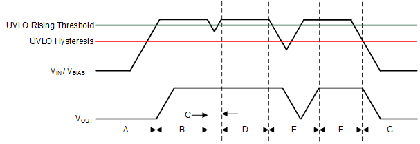
Figure 40 depicts the UVLO circuit response to various input or bias voltage events. This figure can be separated into the following parts:
- Region A: The device does not start until the input or bias voltage reaches the UVLO rising threshold.
- Region B: Normal operation, regulating device
- Region C: Brownout event above the UVLO falling threshold (UVLO rising threshold – UVLO hysteresis). The output may fall out of regulation, but the device is still enabled.
- Region D: Normal operation, regulating device
- Region E: Brownout event below the UVLO falling threshold. The device is disabled in most cases, and the output falls as a result of the load and active discharge circuit. The device is re-enabled when the UVLO rising threshold is reached, and a normal start-up follows.
- Region F: Normal operation followed by the input or bias falling to the UVLO falling threshold
- Region G: The device is disabled as the input or bias voltages fall below the UVLO falling threshold to 0 V. The output falls as a result of the load and active discharge circuit.
 Figure 40. Typical VIN or VBIAS UVLO Circuit Operation