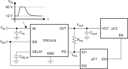
The TPS7A16 family of ultralow power, low-dropout (LDO) voltage regulators offers the benefits of ultra-low quiescent current, high input voltage and miniaturized, high thermal-performance packaging.
The TPS7A16 family is designed for continuous or sporadic (power backup) battery-powered applications where ultralow quiescent current is critical to extending system battery life.
The TPS7A16 family offers an enable pin (EN) compatible with standard CMOS logic and an integrated open drain active-high power good output (PG) with a user-programmable delay. These pins are intended for use in microcontroller-based, battery-powered applications where power-rail sequencing is required.
In addition, the TPS7A16 is ideal for generating a low-voltage supply from multicell solutions ranging from high cell-count power-tool packs to automotive applications; not only can this device supply a well-regulated voltage rail, but it can also withstand and maintain regulation during voltage transients. These features translate to simpler and more cost-effective, electrical surge-protection circuitry.
PART NUMBER | PACKAGE | BODY SIZE (NOM) |
---|---|---|
TPS7A16 | HVSSOP (8) | 3.00 mm × 3.00 mm |
VSON (8) | 3.00 mm × 3.00 mm |
Changes from E Revision (August 2015) to F Revision
Changes from D Revision (January 2014) to E Revision
Changes from C Revision (November 2013) to D Revision
Changes from B Revision (April 2013) to C Revision
Changes from A Revision (December 2011) to B Revision
Changes from * Revision (December 2011) to A Revision
PIN | I/O | DESCRIPTION | |
---|---|---|---|
NAME | NO. | ||
DELAY | 7 | O | Delay pin. Connect a capacitor to GND to adjust the PG delay time; leave open if the reset function is not needed. |
EN | 5 | I | Enable pin. This pin turns the regulator on or off. If VEN ≥ VEN_HI, the regulator is enabled. If VEN ≤ VEN_LO, the regulator is disabled. If not used, the EN pin can be connected to IN. Make sure that VEN ≤ VIN at all times. |
FB/DNC | 2 | I | For the adjustable version (TPS7A1601), the feedback pin is the input to the control-loop error amplifier. This pin is used to set the output voltage of the device when the regulator output voltage is set by external resistors. For the fixed voltage versions: Do not connect to this pin. Do not route this pin to any electrical net, not even GND or IN. |
GND | 4 | GND | Ground pin. |
IN | 8 | IN | Regulator input supply pin. A capacitor ≥ 0.1 µF must be tied from this pin to ground to assure stability. TI recommends connecting a 10-µF ceramic capacitor from IN to GND (as close to the device as possible) to reduce circuit sensitivity to printed-circuit-board (PCB) layout, especially when long input traces or high source impedances are encountered. |
NC | 6 | — | This pin can be left open or tied to any voltage between GND and IN. |
OUT | 1 | O | Regulator output pin. A capacitor ≥ 2.2 µF must be tied from this pin to ground to assure stability. TI recommends connecting a 10-µF ceramic capacitor from OUT to GND (as close to the device as possible) to maximize AC performance. |
PG | 3 | O | Power-good pin. Open collector output; leave open or connect to GND if the power-good function is not needed. |
PowerPAD | — | — | Solder to printed-circuit-board (PCB) to enhance thermal performance. Although it can be left floating, TI highly recommends connecting the PowerPAD to the GND plane. |
MIN | MAX | UNIT | ||
---|---|---|---|---|
Voltage | IN pin to GND pin | –0.3 | 62 | V |
OUT pin to GND pin | –0.3 | 20 | ||
OUT pin to IN pin | –62 | 0.3 | ||
FB pin to GND pin | –0.3 | 3 | ||
FB pin to IN pin | –62 | 0.3 | ||
EN pin to IN pin | –62 | 0.3 | ||
EN pin to GND pin | –0.3 | 62 | ||
PG pin to GND pin | –0.3 | 5.5 | ||
DELAY pin to GND pin | –0.3 | 5.5 | ||
Current | Peak output | Internally limited | ||
Temperature | Operating virtual junction, TJ | –40 | 150 | °C |
Storage, Tstg | –65 | 150 |
VALUE | UNIT | |||
---|---|---|---|---|
V(ESD) | Electrostatic discharge | Human body model (HBM), per ANSI/ESDA/JEDEC JS-001, all pins(1) | ±2000 | V |
Charged device model (CDM), per JEDEC specification JESD22-C101, all pins(2) | ±500 |
MIN | NOM | MAX | UNIT | ||
---|---|---|---|---|---|
VIN | Unregulated input | 3 | 60 | V | |
VOUT | Regulated output | 1.169 | 18.5 | V | |
EN | 0 | 40 | V | ||
DELAY | 0 | 5 | V | ||
PG | 0 | 5 | V | ||
TJ | Operating junction temperature range | –40 | 125 | °C |
THERMAL METRIC(1) | TPS7A1601 | UNIT | ||
---|---|---|---|---|
DGN (HVSSOP) | DRB (VSON) | |||
8 PINS | 8 PINS | |||
RθJA | Junction-to-ambient thermal resistance | 66.2 | 44.5 | °C/W |
RθJC(top) | Junction-to-case(top) thermal resistance | 45.9 | 49.5 | °C/W |
RθJB | Junction-to-board thermal resistance | 34.6 | 11.3 | °C/W |
ψJT | Junction-to-top characterization parameter | 1.9 | 0.7 | °C/W |
ψJB | Junction-to-board characterization parameter | 34.3 | 11.2 | °C/W |
RθJC(bot) | Junction-to-case(bottom) thermal resistance | 14.9 | 4.7 | °C/W |
PARAMETER | TEST CONDITIONS | MIN | TYP | MAX | UNIT | |||
---|---|---|---|---|---|---|---|---|
VIN | Input voltage range | 3 | 60 | V | ||||
VREF | Internal reference | TJ = 25°C, VFB = VREF, VIN = 3 V, IOUT = 10 μA | 1.169 | 1.193 | 1.217 | V | ||
VUVLO | Undervoltage lockout threshold | 2.7 | V | |||||
VOUT | Output voltage range | VIN ≥ VOUT(NOM) + 0.5 V | VREF | 18.5 | V | |||
Nominal accuracy | TJ = 25°C, VIN = 3 V, IOUT = 10 μA | –2% | 2% | VOUT | ||||
Overall accuracy | VOUT(NOM) + 0.5 V ≤ VIN ≤ 60 V(1)
10 µA ≤ IOUT ≤ 100 mA |
–2% | 2% | VOUT | ||||
ΔVO(ΔVI) | Line regulation | 3 V ≤ VIN ≤ 60 V | ±1% | VOUT | ||||
ΔVO(ΔIO) | Load regulation | 10 µA ≤ IOUT ≤ 100 mA | ±1% | VOUT | ||||
VDO | Dropout voltage | VIN = 4.5 V, VOUT(NOM) = 5 V, IOUT = 20 mA | 60 | mV | ||||
VIN = 4.5 V, VOUT(NOM) = 5 V, IOUT = 100 mA | 265 | 500 | mV | |||||
ILIM | Current limit | VOUT = 90% VOUT(NOM), VIN = 3 V | 101 | 225 | 400 | mA | ||
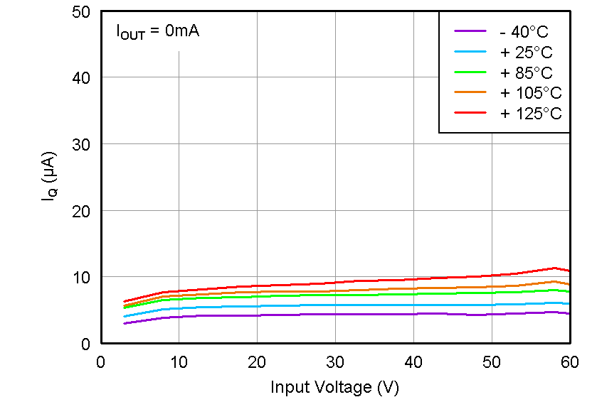
IGND | Ground current | 3 V ≤ VIN ≤ 60 V, IOUT = 10 µA | 5 | 15 | μA | |||
IOUT = 100 mA | 5 | μA | ||||||
ISHDN | Shutdown supply current | VEN = 0.4 V | 0.59 | 5 | μA | |||
I FB | Feedback current(2) | –0.1 | –0.01 | 0.1 | µA | |||
IEN | Enable current | 3 V ≤ VIN ≤ 12 V, VIN = VEN | –1 | –0.01 | 1 | μA | ||
VEN_HI | Enable high-level voltage | 1.2 | V | |||||
VEN_LO | Enable low- level voltage | 0.3 | V | |||||
VIT | PG trip threshold | OUT pin floating, VFB increasing, VIN ≥ VIN_MIN | 85% | 95% | VOUT | |||
OUT pin floating, VFB decreasing, VIN ≥ VIN_MIN | 83% | 93% | VOUT | |||||
VHYS | PG trip hysteresis | 2.3% | 4% | VOUT | ||||
VPG, LO | PG output low voltage | OUT pin floating, VFB = 80% VREF, IPG= 1mA | 0.4 | V | ||||
IPG, LKG | PG leakage current | VPG= VOUT(NOM) | –1 | 1 | μA | |||
IDELAY | DELAY pin current | 1 | 2 | μA | ||||
PSRR | Power-supply rejection ratio | VIN = 3 V, VOUT(NOM) = VREF, COUT = 10 μF, f = 100 Hz |
50 | dB | ||||
TSD | Thermal shutdown temperature | Shutdown, temperature increasing | 170 | °C | ||||
Reset, temperature decreasing | 150 | °C | ||||||
TJ | Operating junction temperature range | –40 | 125 | °C |