JAJSIP6H March 2020 – July 2024 TPS7A20
PRODUCTION DATA
- 1
- 1 特長
- 2 アプリケーション
- 3 概要
- 4 Pin Configuration and Functions
- 5 Specifications
- 6 Detailed Description
- 7 Application and Implementation
- 8 Device and Documentation Support
- 9 Revision History
- 10Mechanical, Packaging, and Orderable Information
パッケージ・オプション
メカニカル・データ(パッケージ|ピン)
サーマルパッド・メカニカル・データ
- DQN|4
発注情報
4 Pin Configuration and Functions
 Figure 4-1 YCJ and YCK
Packages,
Figure 4-1 YCJ and YCK
Packages,4-Pin DSBGA(Top View)
 Figure 4-2 YCJ and YCK
Packages,
Figure 4-2 YCJ and YCK
Packages,4-Pin DSBGA(Bottom View)
Pin Functions: DSBGA
| PIN | I/O | DESCRIPTION | |
|---|---|---|---|
| NO. | NAME | ||
| A1 | IN | I | Input voltage supply. For best transient response and to minimize input impedance, use the nominal value or larger capacitor from IN to ground as listed in the Recommended Operating Conditions table. Place the input capacitor as close to the IN and GND pins of the device as possible. |
| A2 | OUT | O | Regulated output voltage. A low equivalent series resistance (ESR) capacitor is required from OUT to ground for stability. For best transient response, use the nominal recommended value or larger capacitor listed in the Recommended Operating Conditions table. Place the output capacitor as close to the OUT and GND pins of the device as possible. |
| B1 | EN | I | Enable input. A low voltage (< VEN(LOW)) on this input turns the regulator off and discharges the output pin to GND. A high voltage (> VEN(HI)) on this pin enables the regulator output. This pin has an internal 500kΩ pulldown resistor to hold the regulator off by default. When VEN > VEN(HI), the 500kΩ pulldown is disconnected to reduce input current. |
| B2 | GND | — | Common ground. |
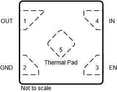
 Figure 4-3 DQN
Package,4-Pin X2SON
(Top View)
 Figure 4-4 DBV
Package,5-Pin SOT-23(Top View)
Figure 4-4 DBV
Package,5-Pin SOT-23(Top View)Pin Functions: X2SON, SOT-23
| PIN | I/O | DESCRIPTION | ||
|---|---|---|---|---|
| NAME | X2SON | SOT-23 | ||
| IN | 4 | 1 | I | Input voltage supply. For best transient response and to minimize input impedance, use the nominal value or larger capacitor from IN to ground as listed in the Recommended Operating Conditions table. Place the input capacitor as close to the IN and GND pins of the device as possible. |
| OUT | 1 | 5 | O | Regulated output voltage. A low equivalent series resistance (ESR) capacitor is required from OUT to ground for stability. For best transient response, use the nominal recommended value or larger capacitor listed in the Recommended Operating Conditions table. Place the output capacitor as close to the OUT and GND pins of the device as possible. An internal 150Ω (typical) pulldown resistor prevents a charge from remaining on VOUT when the regulator is in shutdown mode (VEN< VEN(LOW)). |
| EN | 3 | 3 | I | Enable input. A low voltage (< VEN(LOW)) on this pin turns the regulator off and discharges the output pin to GND. A high voltage (> VEN(HI)) on this pin enables the regulator output. This pin has an internal 500kΩ pulldown resistor to hold the regulator off by default. When VEN > VEN(HI), the 500kΩ pulldown is disconnected to reduce input current. |
| GND | 2 | 2 | — | Common ground. |
| N/C | — | 4 | — | No internal electrical connection. |
| Thermal Pad | 5 | — | — | Thermal pad for the X2SON package. Connect this pad to GND or leave floating. Do not connect to any potential other than GND. Connect the thermal pad to a large-area ground plane for best thermal performance. |