SBVS169D December 2011 – April 2015 TPS7A33
PRODUCTION DATA.
- 1 Features
- 2 Applications
- 3 Description
- 4 Revision History
- 5 Pin Configuration and Functions
- 6 Specifications
- 7 Detailed Description
-
8 Application and Implementation
- 8.1
Application Information
- 8.1.1 Adjustable Operation
- 8.1.2 Capacitor Recommendations
- 8.1.3 Input and Output Capacitor Requirements
- 8.1.4 Noise Reduction and Feed-Forward Capacitor Requirements
- 8.1.5 Post DC-DC Converter Filtering
- 8.1.6 Audio Applications
- 8.1.7 Maximum AC Performance
- 8.1.8 Power-Supply Rejection
- 8.1.9 Output Noise
- 8.1.10 Transient Response
- 8.1.11 Power for Precision Analog
- 8.2 Typical Application
- 8.3 Do's and Don’ts
- 8.1
Application Information
- 9 Power Supply Recommendations
- 10Layout
- 11Device and Documentation Support
- 12Mechanical, Packaging, and Orderable Information
パッケージ・オプション
メカニカル・データ(パッケージ|ピン)
- RGW|20
サーマルパッド・メカニカル・データ
- RGW|20
発注情報
7 Detailed Description
7.1 Overview
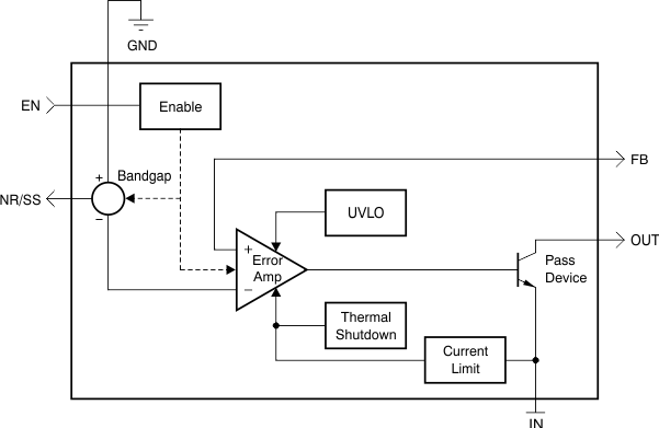
The TPS7A33 belongs to a family of new-generation linear regulators that use an innovative bipolar process to achieve ultralow-noise and very high PSRR levels at a wide input voltage and current range. These features, combined with the external heatsink-capable, high thermal performance TO-220 package, make this device ideal for high-performance analog applications.
7.3 Feature Description
7.3.1 Internal Current Limit
The fixed internal current limit of the TPS7A33xx family helps protect the regulator during fault conditions. The maximum amount of current the device can source is the current limit (1.9 A, typical), and it is largely independent of output voltage. For reliable operation, do not operate the device in current limit for extended periods of time.
7.3.2 Enable Pin Operation
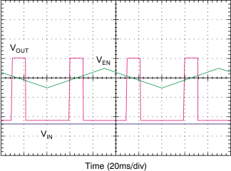
The TPS7A33 provides a dual-polarity enable pin (EN) that turns on the regulator when |VEN| > 2 V, whether the voltage is positive or negative, as shown in Figure 28.
This functionality allows for different system power management topologies; for example:
- Connecting the EN pin directly to a negative voltage, such as VIN, or
- Connecting the EN pin directly to a positive voltage, such as the output of digital logic circuitry.
 Figure 28. Enable Pin Positive and Negative Threshold
7.3.3 Programmable Soft-Start
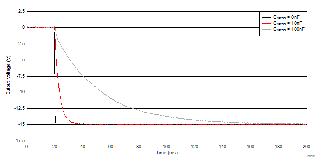
The NR capacitor also acts as a soft-start capacitor to slow down the rise time of the output. The output rise time, when using an NR capacitor, is governed by Equation 1.

In Equation 1, tSS is the soft-start time in milliseconds, and CNR/SS is the capacitance at the NR pin in nanofarads.
Figure 29 shows the start-up voltage waveforms versus CNR/SS.
 Figure 29. Start-Up vs CNR/SS
7.3.4 Thermal Protection
Thermal protection disables the output when the junction temperature rises to approximately 170°C, allowing the device to cool. When the junction temperature cools to approximately 150°C, the output circuitry is enabled. Depending on power dissipation, thermal resistance, and ambient temperature, the thermal protection circuit may cycle on and off. This cycling limits the dissipation of the regulator, protecting it from damage as a result of overheating.
Any tendency to activate the thermal protection circuit indicates excessive power dissipation or an inadequate heat sink. For reliable operation, junction temperature should be limited to a maximum of 125°C. To estimate the margin of safety in a complete design (including heat sink), increase the ambient temperature until the thermal protection is triggered; use worst-case loads and signal conditions. For good reliability, thermal protection should trigger at least 35°C above the maximum expected ambient condition of your particular application. This configuration produces a worst-case junction temperature of 125°C at the highest expected ambient temperature and worst-case load.
The internal protection circuitry of the TPS7A33 has been designed to protect against overload conditions. It was not intended to replace proper heatsinking. Continuously running the TPS7A33 into thermal shutdown degrades device reliability.
7.4 Device Functional Modes
7.4.1 Normal Operation
The device regulates to the nominal output voltage under the following conditions:
- The input voltage has previously exceeded the UVLO rising voltage and has not decreased below the UVLO falling threshold.
- The input voltage is greater than the nominal output voltage added to the dropout voltage.
- |VEN| > |V(HI)|
- The output current is less than the current limit.
- The device junction temperature is less than the maximum specified junction temperature.
7.4.2 Dropout Operation
If the input voltage magnitude is lower than the nominal output voltage magnitude plus the specified dropout voltage magnitude, but all other conditions are met for normal operation, the device operates in dropout mode. In this condition, the output voltage magnitude is the same as the input voltage magnitude minus the dropout voltage magnitude. The transient performance of the device is significantly degraded because the pass device (as a bipolar junction transistor, or BJT) is in saturation and no longer controls the current through the LDO. Line or load transients in dropout can result in large output voltage deviations.
7.4.3 Disabled
The device is disabled under the following conditions:
- |VEN| < |V(HI)|
- The device junction temperature is greater than the thermal shutdown temperature.
Table 1 shows the conditions that lead to the different modes of operation.
Table 1. Device Functional Mode Comparison
| OPERATING MODE | PARAMETER | |||
|---|---|---|---|---|
| VIN | VEN | IOUT | TJ | |
| Normal mode | |VIN| > { |VOUT(nom)| + |VDO|, |VIN(min)| } | |VEN| > |V(HI)| | I OUT < ICL | T J < 125°C |
| Dropout mode | |VIN(min)| < |VIN| < |VOUT(nom)| + |VDO| | |VEN| > |V(HI)| | — | TJ < 125°C |
| Disabled mode (any true condition disables the device) |
— | |VEN| < |V(HI)| | — | TJ > 165°C |
