JAJSEV1A September 2017 – February 2018 TPS7A54-Q1
PRODUCTION DATA.
- 1 特長
- 2 アプリケーション
- 3 概要
- 4 改訂履歴
- 5 Pin Configuration and Functions
- 6 Specifications
- 7 Detailed Description
-
8 Application and Implementation
- 8.1
Application Information
- 8.1.1 Recommended Capacitor Types
- 8.1.2 Soft Start and Inrush Current
- 8.1.3 Optimizing Noise and PSRR
- 8.1.4 Charge Pump Noise
- 8.1.5 Current Sharing
- 8.1.6 Adjustable Operation
- 8.1.7 Power-Good Operation
- 8.1.8 Undervoltage Lockout (UVLO) Operation
- 8.1.9 Dropout Voltage (VDO)
- 8.1.10 Device Behavior During Transition From Dropout Into Regulation
- 8.1.11 Load Transient Response
- 8.1.12 Reverse Current Protection Considerations
- 8.1.13 Power Dissipation (PD)
- 8.1.14 Estimating Junction Temperature
- 8.2 Typical Application
- 8.1
Application Information
- 9 Power Supply Recommendations
- 10Layout
- 11デバイスおよびドキュメントのサポート
- 12メカニカル、パッケージ、および注文情報
パッケージ・オプション
メカニカル・データ(パッケージ|ピン)
- RGR|20
サーマルパッド・メカニカル・データ
- RGR|20
発注情報
8.1.12 Reverse Current Protection Considerations
As with most LDOs, this device can be damaged by excessive reverse current.
Conditions where excessive reverse current can occur are outlined in this section, all of which can exceed the absolute maximum rating of VOUT > VIN + 0.3 V:
- If the device has a large COUT, then the input supply collapses quickly and the load current becomes very small
- The output is biased when the input supply is not established
- The output is biased above the input supply
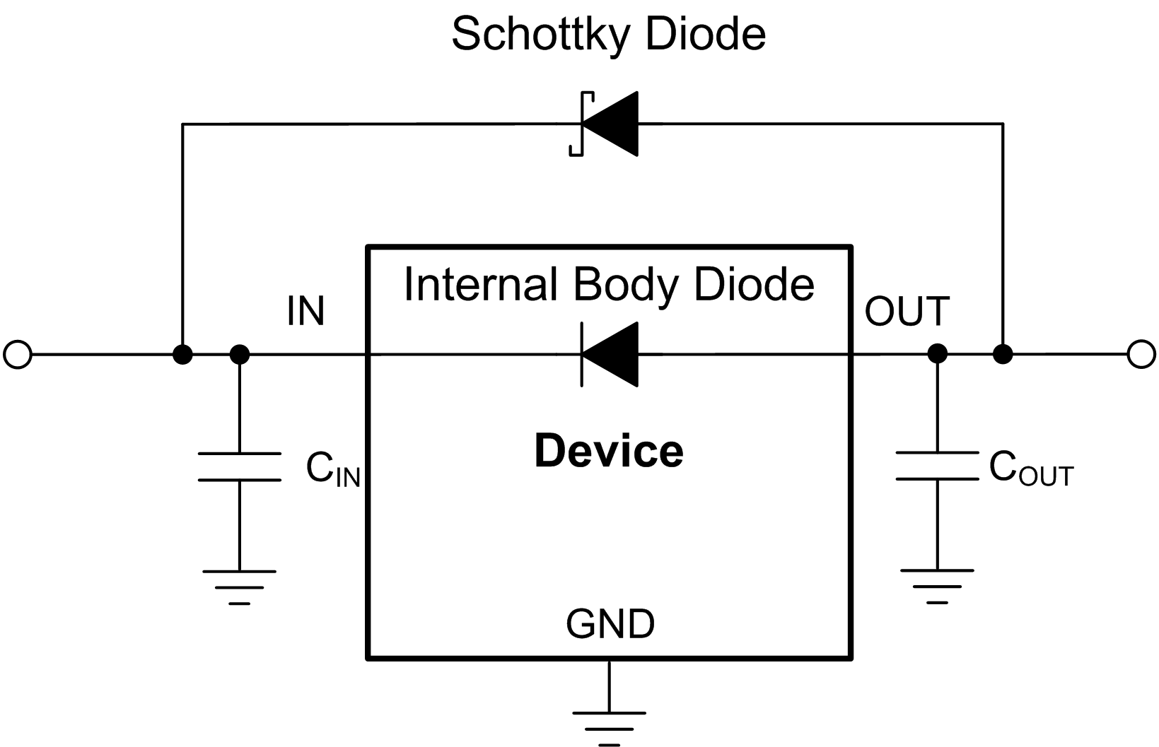
If an excessive reverse current flow is expected in the application, then external protection must be used to protect the device. Figure 46 shows one approach of protecting the device.
 Figure 46. Example Circuit for Reverse Current Protection Using a Schottky Diode